Programmable in-situ delay fault test clock generator

a clock generator and delay technology, applied in the direction of generating/distributing signals, pulse techniques, instruments, etc., can solve the problems of increasing the number of failures caused by defects in the manufacturing process and design margins, the ineffectiveness of conventional fault testing methods such as stuck fault models, etc., and the difficulty of maintaining the accuracy of these clocks at higher clock speeds

Active Publication Date: 2009-05-19
CISCO TECH INC
View PDF6 Cites 14 Cited by
  • Summary
  • Abstract
  • Description
  • Claims
  • Application Information

AI Technical Summary

Problems solved by technology

As the geometries of semiconductor devices are getting smaller, failures caused by defects in the manufacturing process and design margins are becoming increasingly common.
Conventional methods of fault testing, such as stuck-at fault models, etc., are no longer an effective solution.
However, maintaining the accuracy of these clocks at higher clock speeds is very costly and difficult.
However, existing test clock generation techniques are not applicable across different technologies, since it is difficult to scale the delay of the clock according to the device requirement.
This reduces the accuracy of testing these devices.
Moreover, these techniques do not address critical path delay measurement.

Method used


Image

  • Programmable in-situ delay fault test clock generator
  • Programmable in-situ delay fault test clock generator
  • Programmable in-situ delay fault test clock generator

Examples


Embodiment Construction

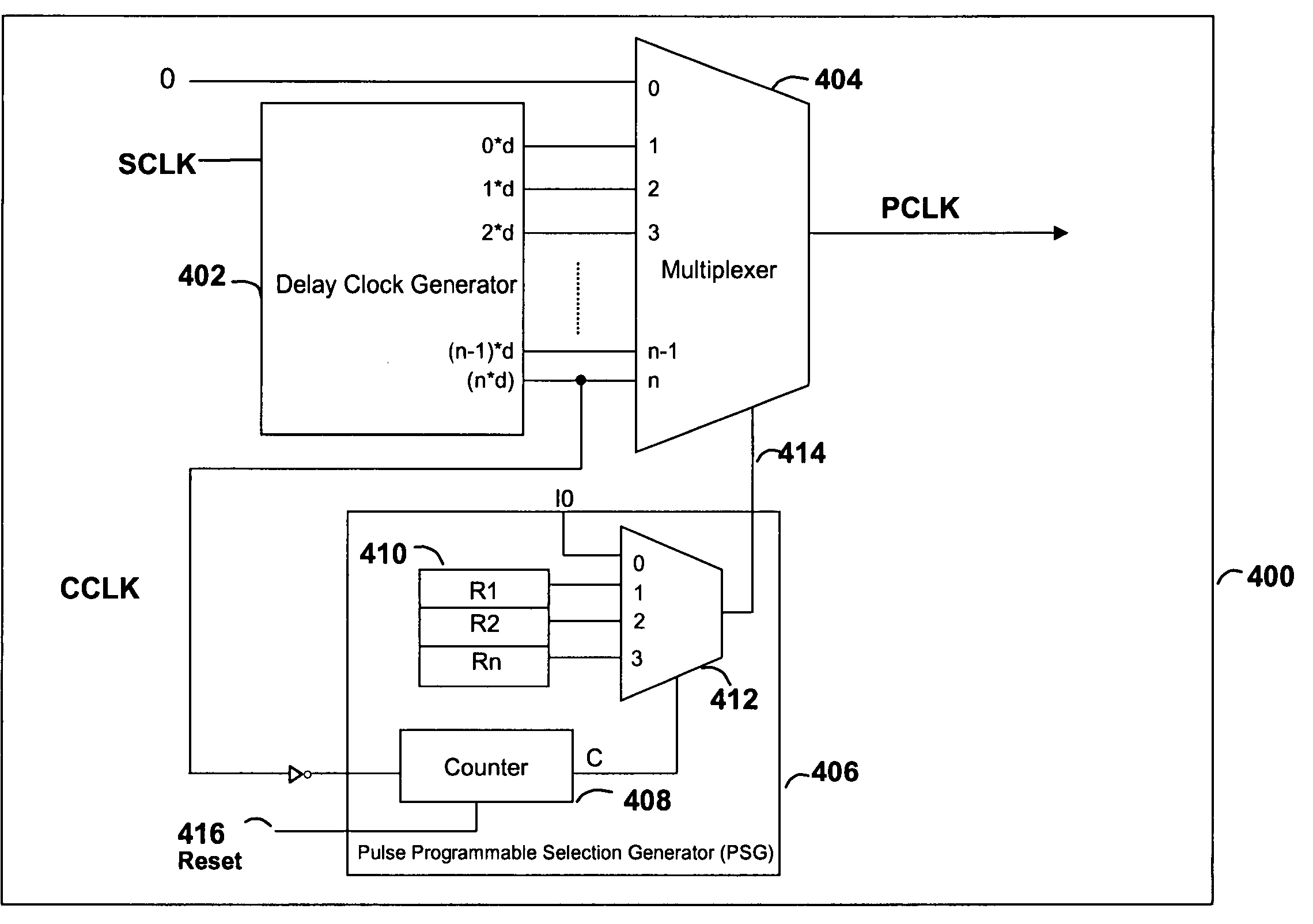
[0019]Various embodiments of the invention provide a system and method for in-situ launch and capture clock generation. In-situ capture and launch clocks are used to test, diagnose and analyze defects in electronic circuits such as semiconductor devices. They also eliminate external tester dependency. The clocks can be used for testing path delay faults and transition faults at any stage of device production and characterization. The embodiments of the invention can be applied across different technologies, starting from a wafer probe station to a system environment, and therefore, have wide applicability.

[0020]In an exemplary embodiment of the invention, a system for generating a launch and capture clock is provided. The system includes i) an in-situ delayed clock generator for generating one or more clocks; ii) a pulse Programmable Selection Generator (PSG) for generating the sequence in which the clocks are to be selected, the clocks being selected with a delay; and iii) a multip...


PUM


Abstract

A system and method for programmable in-situ launch and capture clock generation is provided. The system provides an efficient and improved manner for delay and signal transition fault testing in electronic circuits. The system comprises i) an in-situ delay clock generator for generating one or more clocks; ii) a pulse Programmable Selection Generator (PSG) which can be either a pulse PSG and / or an expanded pulse PSG for generating the sequence in which the clocks are to be selected, the clocks being selected with a delay; and iii) a multiplexer for selecting the plurality of clocks, based on the generated sequence, the selected clocks being used for generating the launch and capture clocks.

Description

BACKGROUND OF THE INVENTION[0001]1. Field of Invention[0002]Embodiments of the present invention relate to fault testing in electronic circuits. More particularly, the embodiments of the present invention relate to programmable in-situ launch and capture clock generation for at-speed testing.[0003]2. Description of the Background Art[0004]Investigating faults in semiconductor devices is a critical aspect of the manufacturing and maintenance process. As the geometries of semiconductor devices are getting smaller, failures caused by defects in the manufacturing process and design margins are becoming increasingly common. Exemplary failures include those caused by timing-related at-speed faults.[0005]Conventional methods of fault testing, such as stuck-at fault models, etc., are no longer an effective solution. A better method is at-speed testing, i.e., testing the device at its working frequency. At-speed testing is based on a transition fault model and / or a path delay fault model. Th...

Claims


Application Information

Patent Timeline
Patent Type & Authority Patents(United States)
IPC IPC(8): G01R31/28
CPCG06F1/06H03K5/133
Inventor JUN, HONG-SHINCHUNG, SUNG SOOKIM, HEONG
Owner CISCO TECH INC
Why Eureka
Try Eureka