Method of forming double gate transistors having varying gate dielectric thicknesses

a dielectric thickness and gate technology, applied in the field of semiconductor devices, can solve the problems of increasing adverse short channel effects, reducing the gain of drive current, and difficult to build a simple, manufacturable planar double gate fdsoi transistor structure,

Active Publication Date: 2009-05-26
TAIWAN SEMICON MFG CO LTD
View PDF17 Cites 33 Cited by
  • Summary
  • Abstract
  • Description
  • Claims
  • Application Information

AI Technical Summary

Problems solved by technology

In addition, scaled down conventional bulk silicon MOSFET devices tend to have diminished gain in drive currents while having increased adverse short channel effects.
However, it has been difficult to build a simple, manufacturable planar double gate FDSOI transistor structure that can be used to fabricate transistors in differing applications.

Method used


Image

  • Method of forming double gate transistors having varying gate dielectric thicknesses
  • Method of forming double gate transistors having varying gate dielectric thicknesses
  • Method of forming double gate transistors having varying gate dielectric thicknesses

Examples


Embodiment Construction

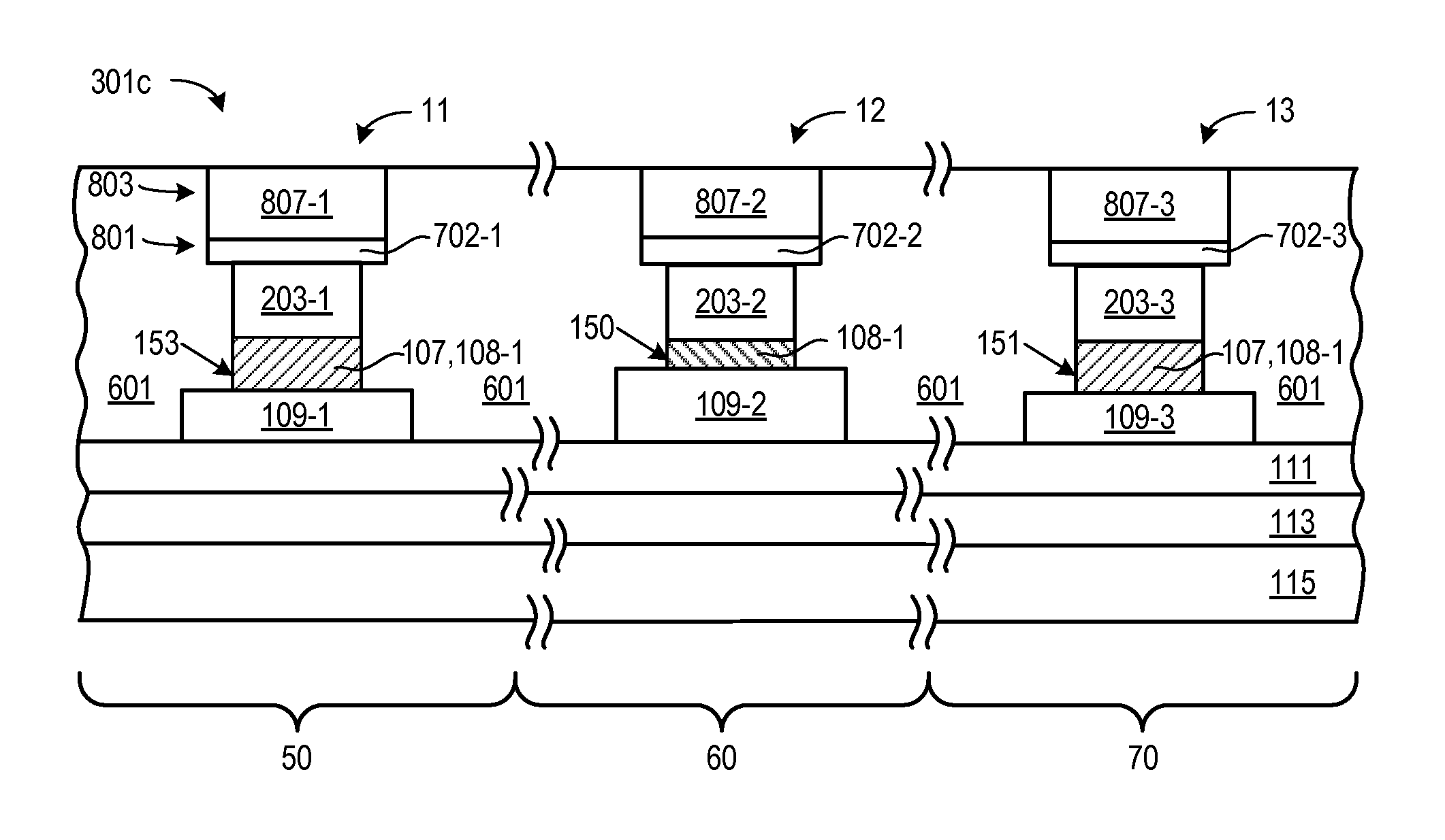
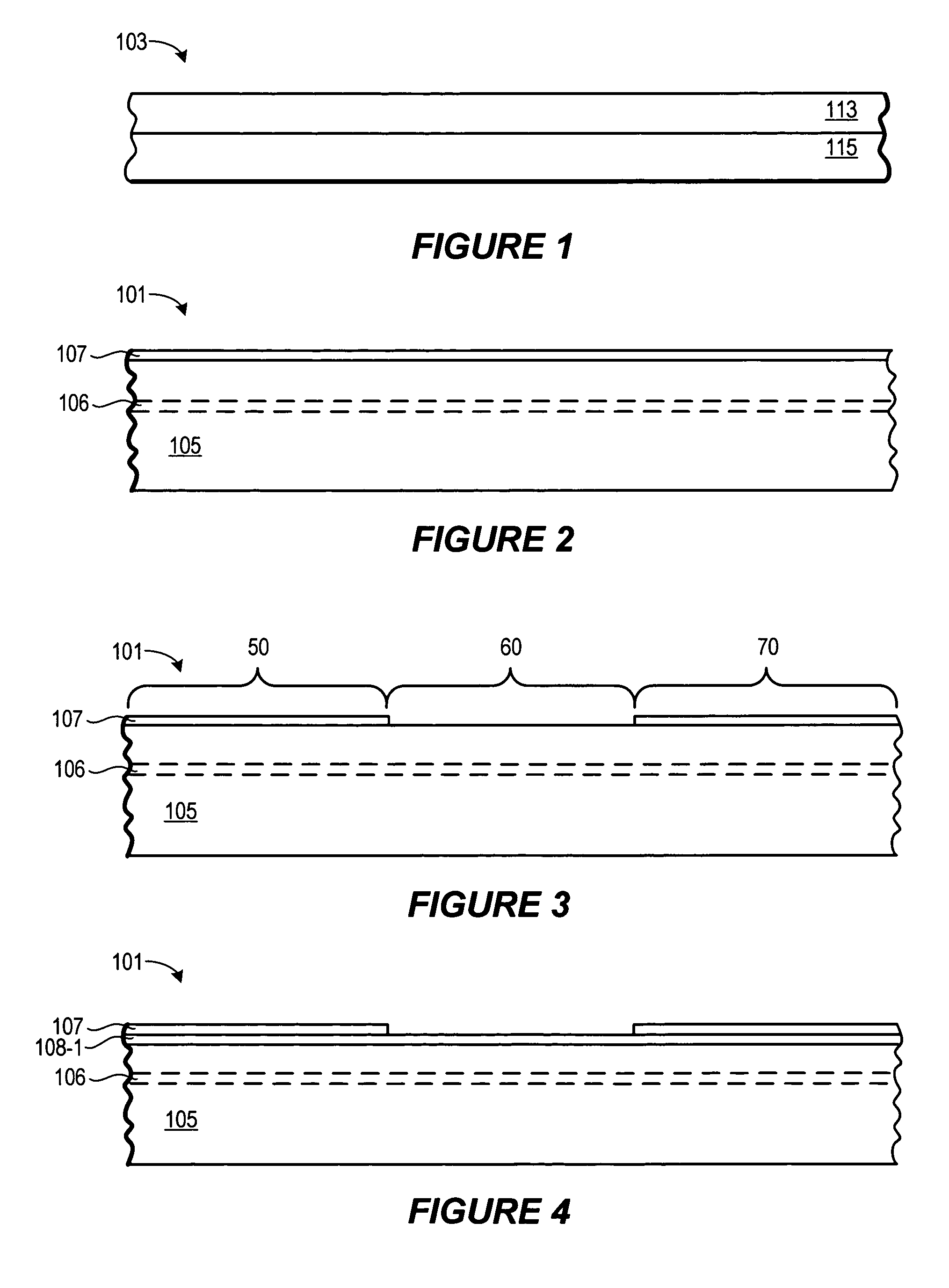
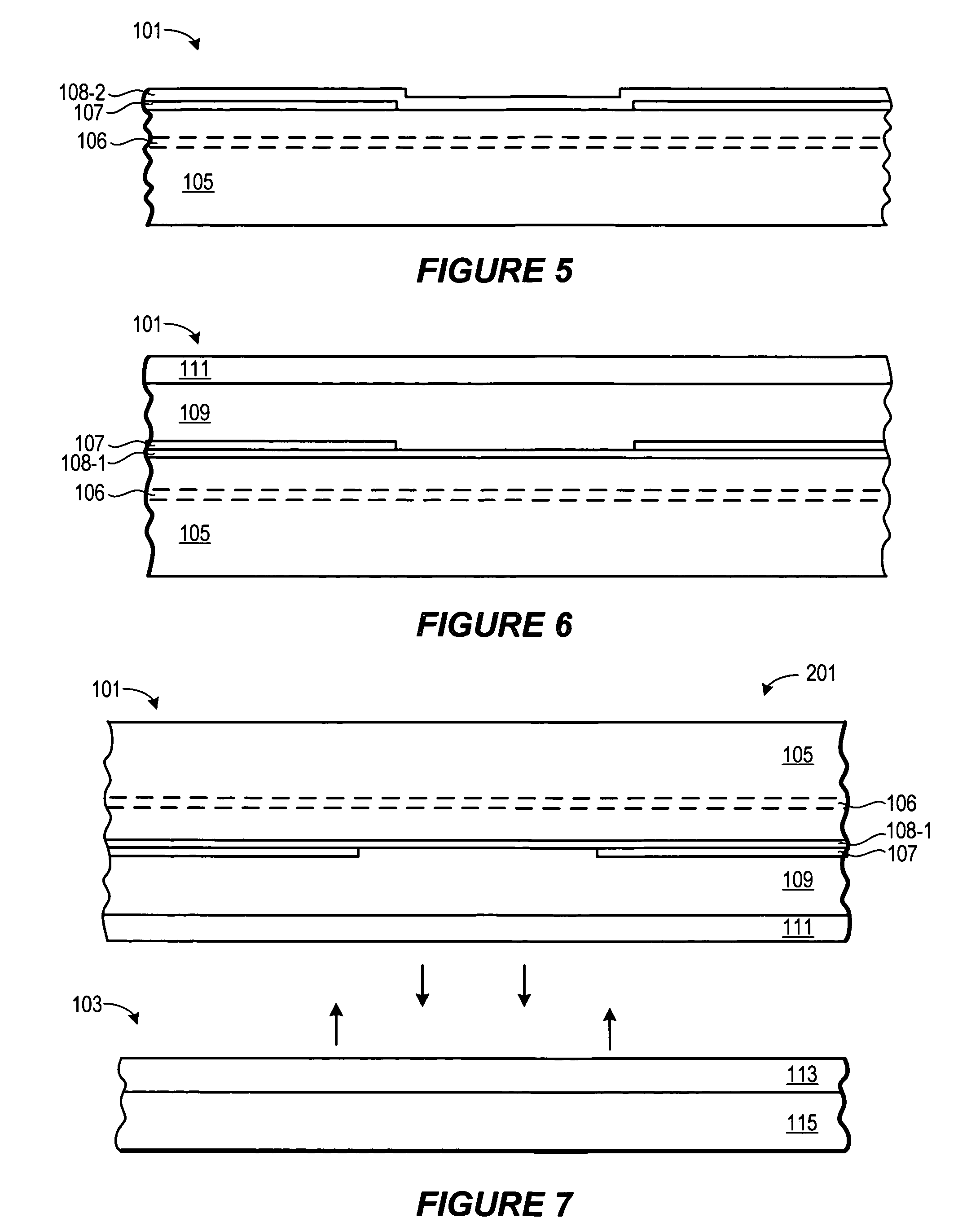
[0025]A method and apparatus are described for fabricating planar double gate devices having multiple possible gate dielectric thicknesses so that, for example, double gate devices used in one part of an integrated circuit have a first bottom gate dielectric, a first bottom gate conductor and an optional first top gate dielectric layer and first top gate conductor layer, while double gate devices used in another part of an integrated circuit have a second bottom gate dielectric, a second bottom gate conductor and an optional second top gate dielectric layer and second top gate conductor layer. While various details are set forth in the following description, it will be appreciated that the present invention may be practiced without these specific details, and that numerous implementation-specific decisions may be made to the invention described herein to achieve the device designer's specific goals, such as compliance with process technology or design-related constraints, which will...


PUM


Abstract

Double gate transistors (12, 13) having different bottom gate dielectric thicknesses are formed on a first wafer (101) by forming a first gate dielectric layer (107); removing part of the first gate dielectric layer (107) from a first area (60); forming a second gate dielectric layer (108) to obtain a thinner bottom gate dielectric layer (150) over the first area (60) and a thicker bottom gate dielectric layer (151) over the second area (70); and forming a planar bottom gate layer (109) over first and second gate dielectric layers. After inverting and bonding the first wafer (101) to a second wafer (103), the bottom gate electrodes (109-2, 109-3), bottom gate dielectric layers (107, 108) and channel regions (203-2, 203-3) for the first and second double gate transistors (12, 13) are selectively etched prior to formation of the top gate structures.

Description

BACKGROUND OF THE INVENTION[0001]1. Field of the Invention[0002]The present invention is directed in general to the field of semiconductor devices. In one aspect, the present invention relates to gate dielectric layers formed on integrated circuit devices.[0003]2. Description of the Related Art[0004]As the size of semiconductor device is scaled down, the requirements for device design and fabrication—such as controlling the thickness of thin gate dielectric and other constituent layers and / or obtaining desired dielectric film composition—continue to be tightened. In addition, scaled down conventional bulk silicon MOSFET devices tend to have diminished gain in drive currents while having increased adverse short channel effects. Double gate Fully Depleted Semiconductor-on-Insulator (FDSOI) technology has been established as one solution to reduce short channel effect as well as to improve drive current (high transconductance). In addition, double gate FDSOI technology may require a le...

Claims


Application Information

Patent Timeline
Patent Type & Authority Patents(United States)
IPC IPC(8): H01L21/336
CPCH01L21/84H01L27/1203H01L29/4908H01L29/78648
Inventor DAO, THUY B.
Owner TAIWAN SEMICON MFG CO LTD
Why Eureka
Try Eureka