Interferometer

an electron interferometer and phase-splitting technology, applied in the field of phase-splitting electron interferometers, can solve the problems of inability of interferometer to control the fringe spacing s and the interference width w independently, and achieve the effect of increasing the range of objects to be observed with holography

Active Publication Date: 2009-05-26
RIKEN
View PDF5 Cites 13 Cited by
  • Summary
  • Abstract
  • Description
  • Claims
  • Application Information

AI Technical Summary

Benefits of technology

[0014]According to the present invention, each of two parameters of a fringe spacing s and an interference width W in interferometry using a biprism can be controlled independently. With this feature, it is possible to independently treat spatial coherence and a carrier-spatial frequency, each directly relating to the performance of an interferometer. As a result, the range of an object to be observed with holography can be increased. Especially, in an electron interferometer, the two parameters of a fringe spacing s and an interference width W can freely and independently be controlled only by controlling voltages to each of upper and lower electron biprisms.

Problems solved by technology

This is because there is no effective amplitude-splitting type beam splitter for an electron beam.
However, this type of interferometer cannot control each of a fringe spacing s and an interference width W independently because of its operational principles.
On the contrary, even if a specimen is small and an interference image obtained in a narrow area with a high carrier-spatial frequency is required for analysis, when a necessary high carrier-spatial frequency is produced, the interference width becomes larger with the spatial coherence deteriorated.
Due to some characteristics (for example, an optical system with only several convex lenses, and an optical system without a half mirror) of electron optical systems, however, there are limitations such as a limitation where the magnification finally obtained is low.
In addition, when a hologram is reconstructed and a phase image is extracted, the Fresnel diffraction waves caused by a breakage at the wavefront generate fringes with strong contrast (Fresnel fringes), which generates artifact in the result of the measurement and impedes high precision phase measurement.
These methods are not sufficient.
This method, however, would not provide any improvement of the primary problem that each of fringe spacing s and interference width W cannot be controlled independently.

Method used


Image

  • Interferometer
  • Interferometer
  • Interferometer

Examples


Embodiment Construction

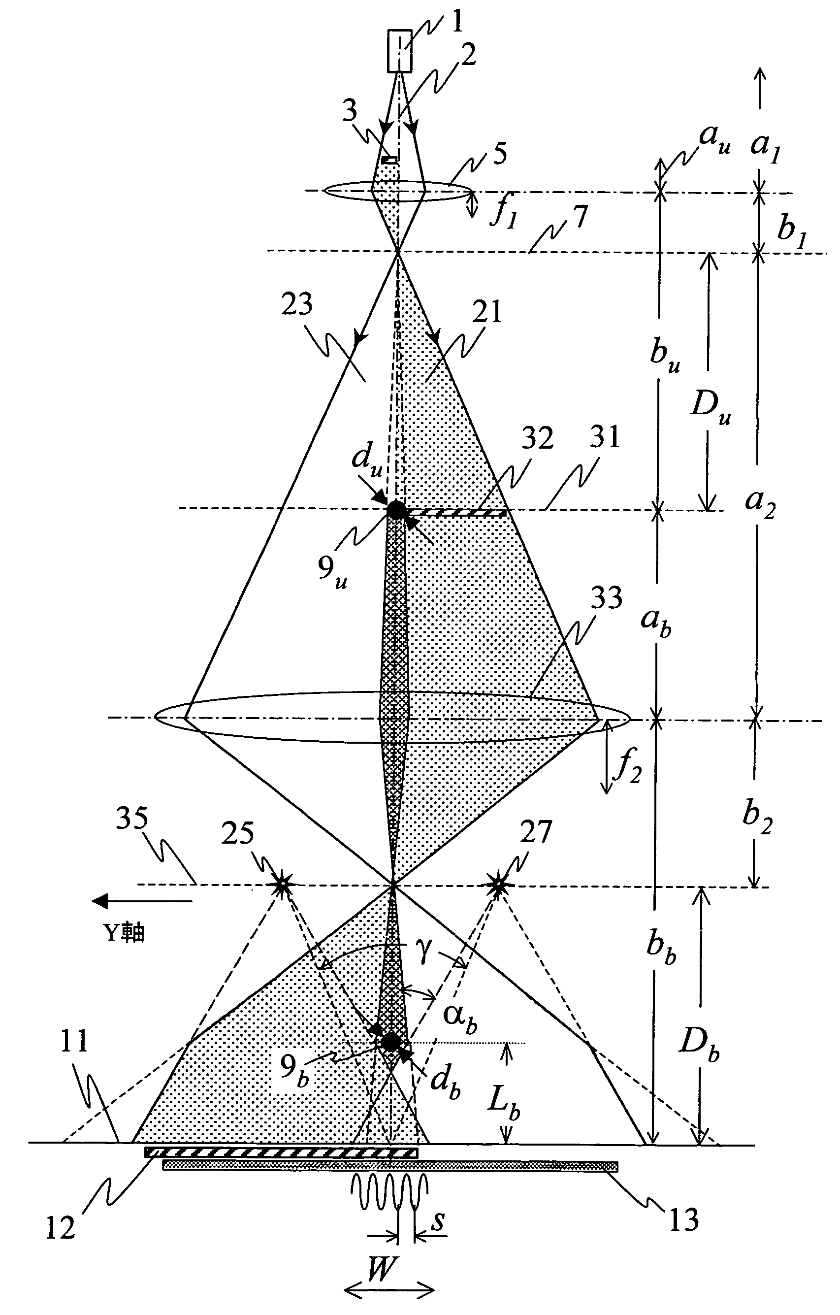
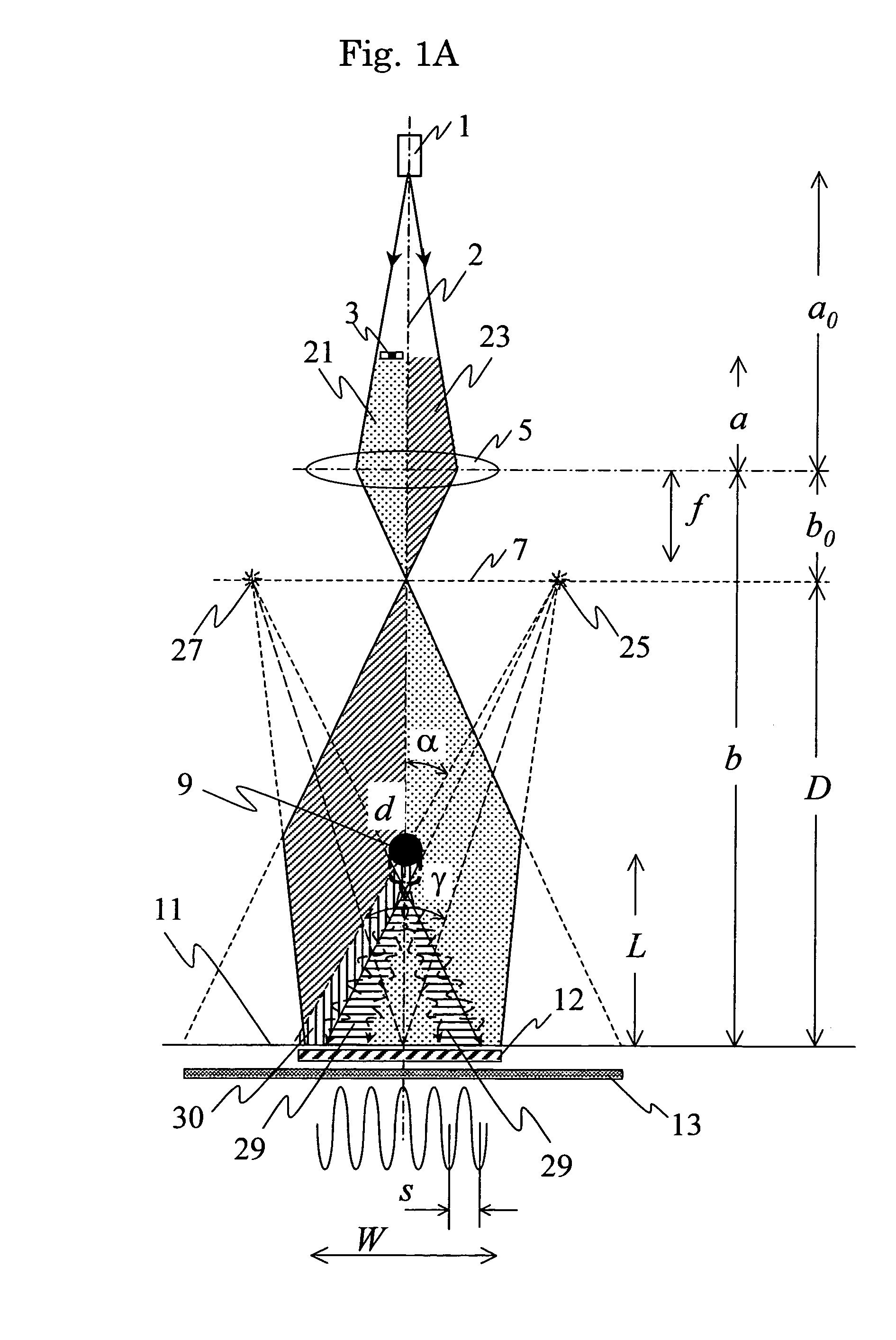
[0098]The present invention is applicable to an electron interferometer and a phase-split type optical interferometer having a general optical biprism. In an embodiment of the present invention described below, however, an electron interferometer is mainly described, and a phase-splitting type optical interferometer having a general optical biprism is described in general in the final section of this specification.

[0099]FIG. 1A is a view illustrating an interference system using an electron beam biprism based on the conventional technology. An electron biprism is a device which is used most popularly as an optical system for electron holography. Reference wave 23 are overlaid on object wave 21 in the optical system. As a result, an interferogram in which interference fringes are superposed on an enlarged image of a specimen is obtained. As well known, the electron biprism has a filament electrode provided at a central portion thereof and double-plates electrodes holding the filament...


PUM


Abstract

The present invention provides a technique enabling to control fringe spacing s and an interference width W independently of each other, which are important parameters for an interferometer using an electron biprism.In the present invention, two electron biprisms 9u, 9b are used in two stages along the optical axis, and fringe spacing s and an interference width W are controlled independently of each other by controlling a voltage applied to an electrode of each of the electron biprisms. Also Fresnel diffraction can be suppressed.

Description

[0001]This application is the US national phase of international application PCT / JP2005 / 000111 filed 7 Jan. 2005, which designated the U.S. and claims priority to JP 2004-004156 filed 9 Jan. 2004, the entire content of each of which is hereby incorporated by reference.TECHNICAL FIELD[0002]The present invention relates to a phase-splitting type electron interferometer having an electron biprism and a phase-splitting type optical interferometer having an optical biprism.BACKGROUND OF THE INVENTION[0003]Optical interferometers are largely classified into those based on an amplitude-splitting method and those based on a phase-splitting method. Excluding specific cases, an optical interferometer (such as that based on a laser) generally employs an amplitude-splitting method. This is because a phase distortion caused by an optical system can be compensated and thereby it becomes relatively easy to accurately detect a minute phase distribution which is an object to be observed. On the othe...

Claims


Application Information

Patent Timeline
Patent Type & Authority Patents(United States)
IPC IPC(8): G01B15/00G01B9/02H01J37/305H01J37/295
CPCH01J37/295H01J2237/1514H01J2237/2614
Inventor HARADA, KENAKASHI, TETSUYATOGAWA, YOSHIHIKOMATSUDA, TSUYOSHIMORIYA, NOBORU
Owner RIKEN
Why Eureka
Try Eureka