

Compound semiconductor FET
a technology of semiconductor fet and semiconductor fet, which is applied in the direction of semiconductor devices, electrical apparatus, transistors, etc., can solve the problems of unresolved causes, and achieve the effect of solving or reducing parallel conduction and gate leakag
- Summary
- Abstract
- Description
- Claims
- Application Information
AI Technical Summary
Benefits of technology
Problems solved by technology
Method used
Image

Examples
first embodiment
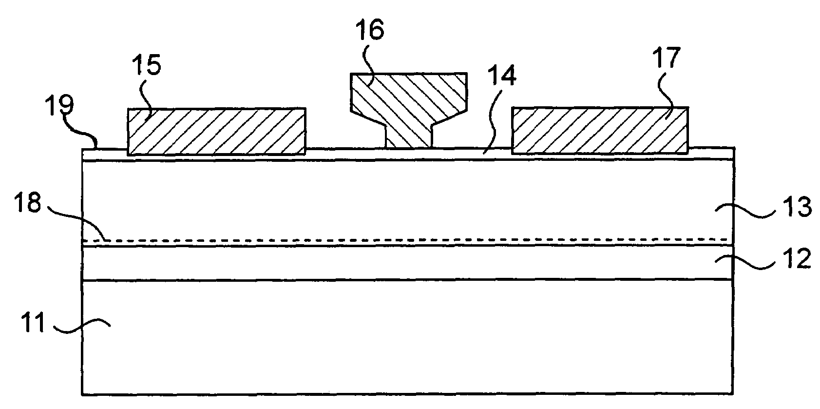
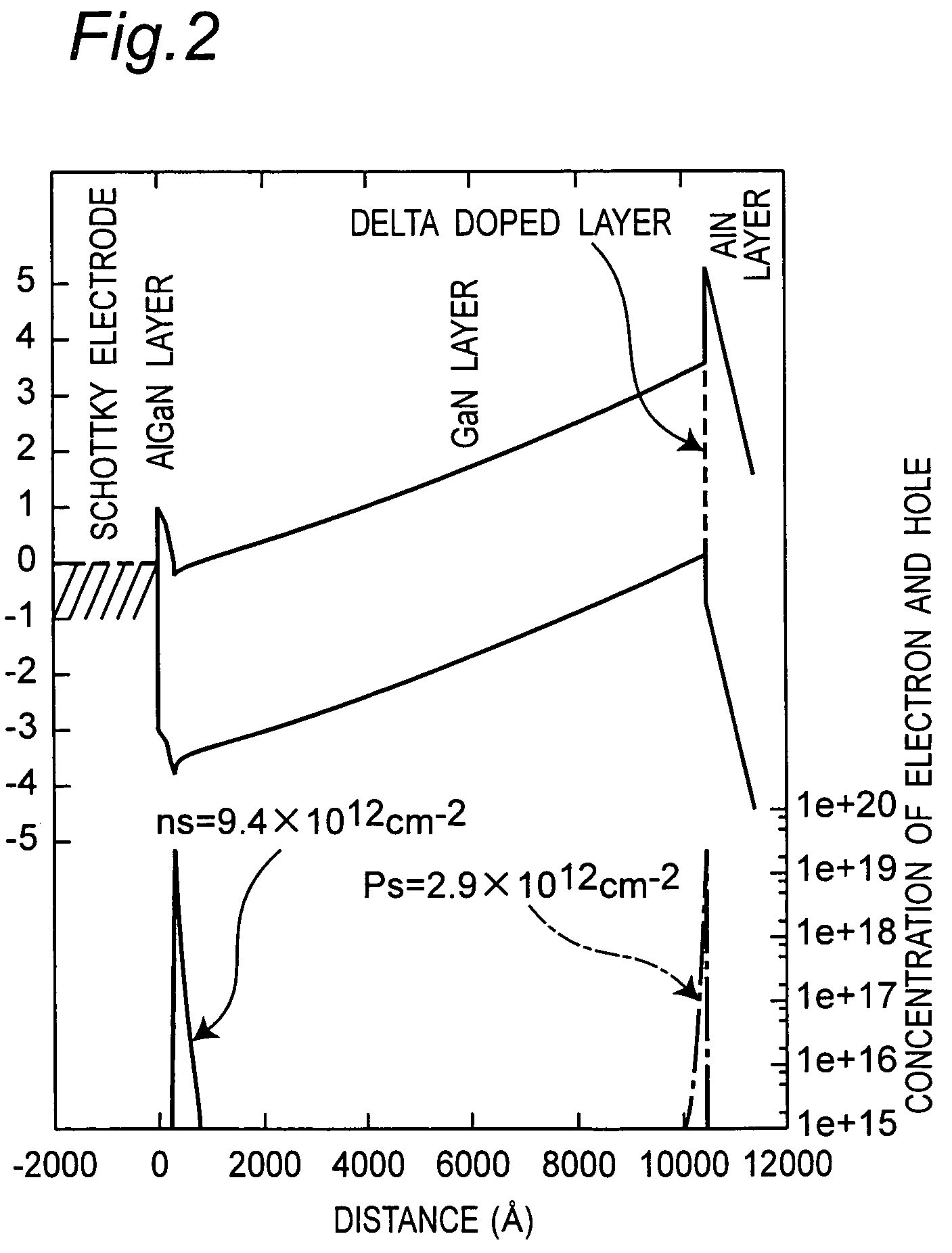
[0034]In FIG. 1, a structure of a GaN HFET according to a first embodiment of the invention is shown. In the semiconductor layers and metal layers shown in FIG. 1, reference numeral 11 denotes a substrate, 12 denotes a 100 nm thick undoped AlN layer, 18 denotes a GaN delta doped layer (with sheet doping concentration ns=1.5×1013 cm−2), 13 denotes a 1 μm thick undoped GaN layer, 14 denotes a 30 nm thick undoped Al0.2Ga0.8N layer, 15 denotes a Ti / Al / Pt / Au based source ohmic electrode, 16 denotes a Pt / Au based gate Schottky electrode, and 17 denotes a Ti / Al / Pt / Au based drain ohmic electrode.
[0035]The present invention features in that the GaN delta doped layer 18 is placed at the interface between the undoped AlN layer 12 and the undoped GaN layer 13. The term “delta doped layer” refers to a layer in which dopants are doped in an extremely thin layer. The thickness of the delta doped layer 18 is ideally 0 nm but actually the layer has some degree of thickness. In the present invention,...
second embodiment
[0045]A GaN HFET of a second embodiment of the present invention has a similar construction to that of the first embodiment shown in FIG. 1 except that the material of the substrate 11 is SiC, that the method of growth of semiconductor layers is the metal-organic chemical vapor deposition (MOCVD), that the thickness of the undoped GaN layer 13 is 2 μm, and that the sheet doping concentration of the GaN delta doped layer 18 is 1.0×1013 cm−2. Simulation results were similar to those of the first embodiment.
third embodiment
[0046]FIG. 4 shows the construction of a GaN HFET according to a third embodiment. The growth method for semiconductor layers in the third embodiment is MBE, and an undoped GaN layer 73 is of the C-plane Ga-surface type. The undoped GaN layer 73 is so thin as 0.75 μm that the cost for growth is reduced. In the structure of the conventional HFET shown in FIG. 7, when the GaN layer is thin like this, the problems of “parallel conduction” and “gate leak” become particularly noticeable.
[0047]In semiconductor layers and metal layers of this GaN HFET, reference numeral 71 denotes a sapphire substrate, 72 denotes a 50 nm thick undoped AlN layer, 78 denotes a GaN delta doped layer (with sheet doping concentration Ns=1.9×1013 cm−2), 73 denotes a 0.75 μm thick undoped GaN layer, 74 denotes a 50 nm thick undoped Al0.2Ga0.8N layer, 75 denotes a Ti / Al / Pt / Au source ohmic electrode, 76 denotes a Pt / Au gate Schottky electrode, and 77 denotes a Ti / Al / Pt / Au drain ohmic electrode.
[0048]The thickness o...
PUM
 Abstract
Description
Claims
Application Information