Silicon-based tunneling field effect transistors and transistor circuitry employing same

a tunneling field effect transistor and transistor technology, applied in the field of electronic circuitry arts, electronic devices, electrical equipment, transistors, etc., can solve the problems of limiting the low-voltage operation of cmos circuitry, power consumption, speed of cmos circuitry, and approaching certain fundamental limits of channel length and power consumption

Active Publication Date: 2012-08-09
THE OHIO STATES UNIV
View PDF2 Cites 22 Cited by
  • Summary
  • Abstract
  • Description
  • Claims
  • Application Information

AI Technical Summary

Problems solved by technology

However, CMOS technology is believed to be approaching certain fundamental limits with respect to channel length, power consumption, steep subthreshold slopes, and related aspects such as leakage current and defect effects that may impose limits on the speed of CMOS circuitry.
These limitations are considered to be consequences of the rather complex material formulation of CMOS which combines electronic conductor, dielectric, and semiconductor materials, with the primary electrical current flowing laterally along and proximate to the dielectric / semiconductor interface.
Diffusion-based current transport is limited by thermal broadening and sets a limit upon CMOS transistor subthreshold slopes of 60 mV per decade of current, which in turn restricts their low-voltage operation.
As chip power consumption has become a premium challenge, a shift towards lower drive voltages mitigates some power losses, but now a physical barrier exists for conventional CMOS.
However, in the unbiased state there is little or no excess charge available proximate to the junction.
As a consequence, turn-on voltage is undesirably high.
Further, the p-channel operating mode does not exhibit drain current (ID) saturation, which limits applicability in digital circuitry and leads to asymmetry between the performance of the p-channel and n-channel.
The lack of truly symmetric n-channel and p-channel devices also constrains the ability to mimic the complementary transistor circuitry of CMOS technology in this TFET system.
However, these p+-SiGe / i-silicon / n-silicon diode TFETs also have problems.

Method used


Image

  • Silicon-based tunneling field effect transistors and transistor circuitry employing same
  • Silicon-based tunneling field effect transistors and transistor circuitry employing same
  • Silicon-based tunneling field effect transistors and transistor circuitry employing same

Examples


Embodiment Construction

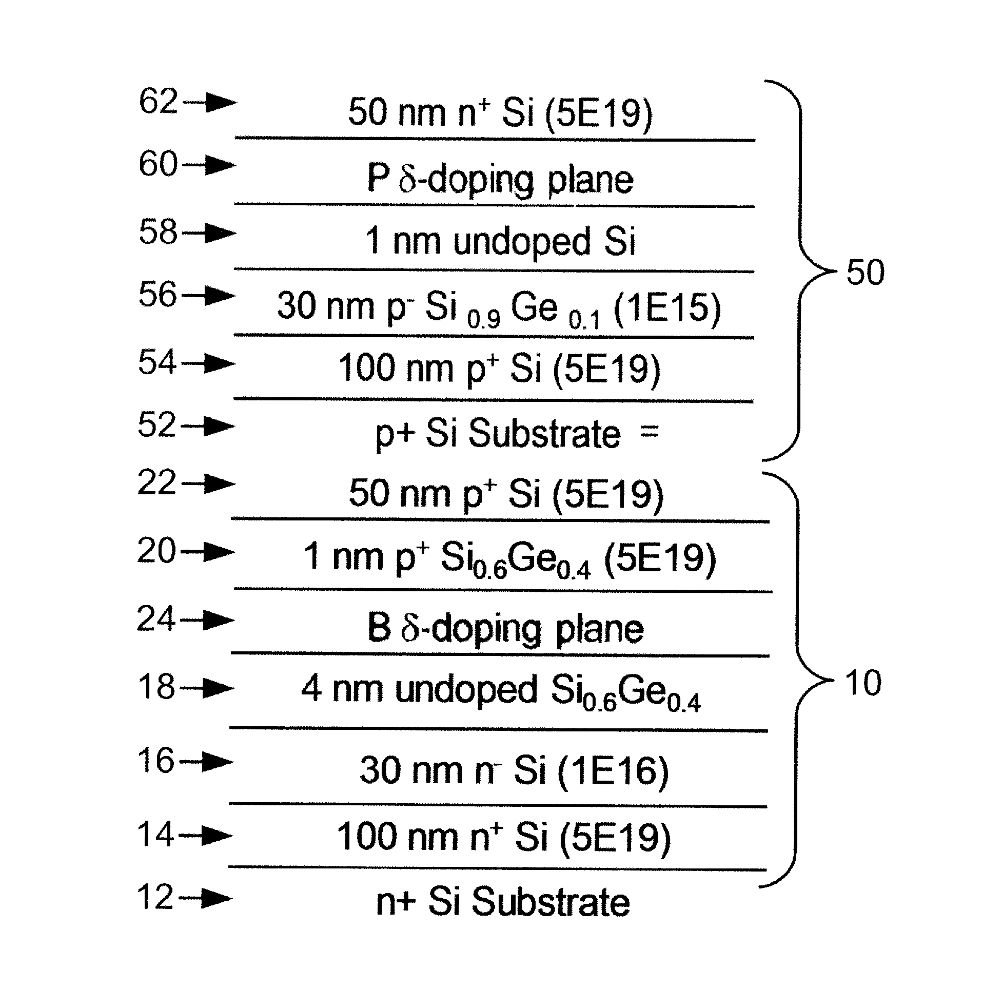
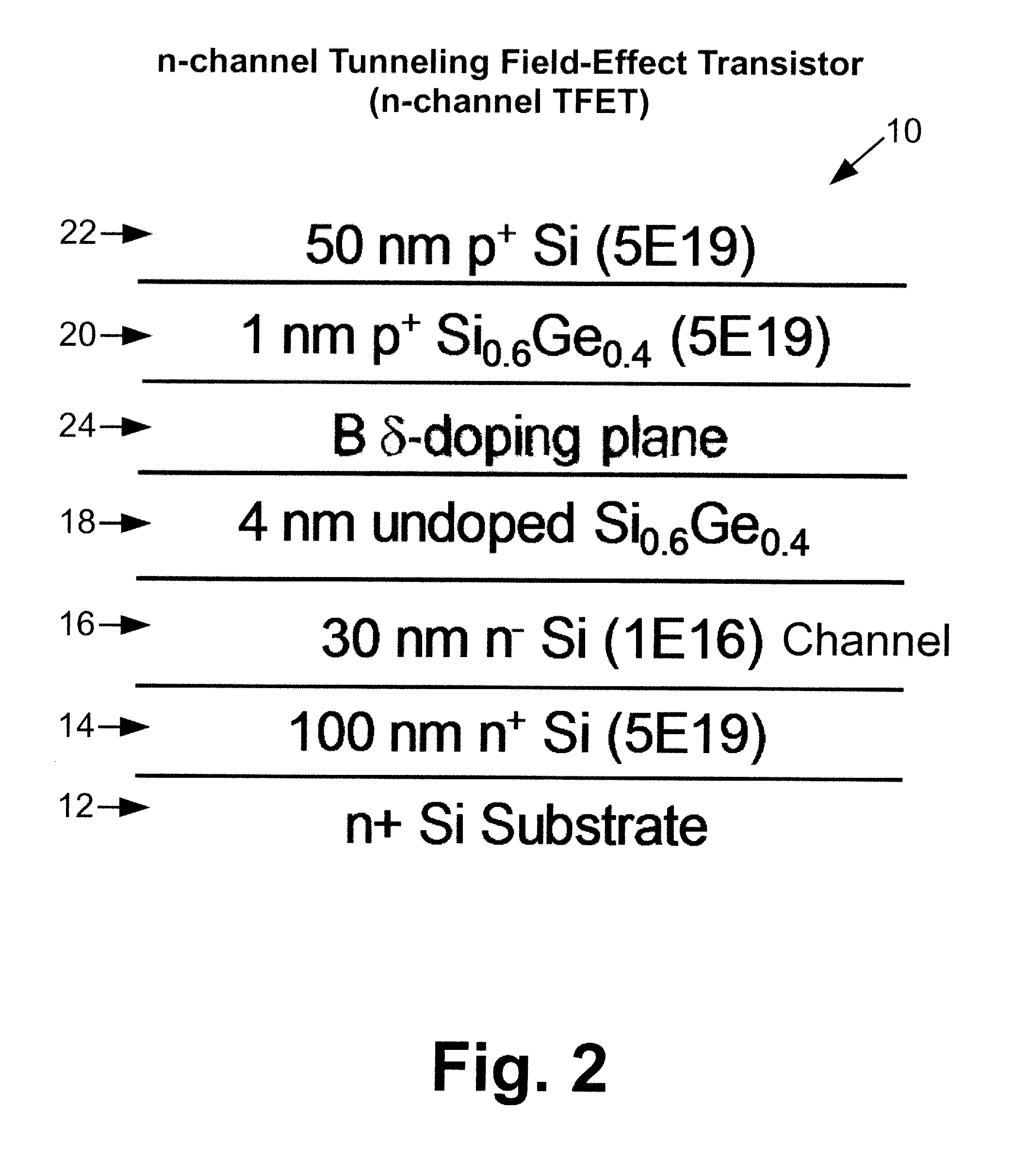
[0031]With reference to FIGS. 1-3, an illustrative n-channel tunneling field-effect transistor (n-channel TFET) 10 is described. FIG. 1 provides an illustrative layer structure including illustrative doping levels (in cm−2, denoted “cm-2” in some drawings) and layer thicknesses (in angstroms, denoted “ang” in some drawings), while FIG. 2 provides a simplified layer structure setting forth salient features in thickness units of nanometers and doping concentrations in cm−3. The illustrative n-channel TFET is formed on an n+ silicon substrate 12, with an optional growth quality-enhancing n+ silicon buffer 14 grown thereon, thus defining an n-type region of the n-channel TFET. This followed by formation of a channel region 16 which in the illustrated embodiment is 30 nm thick and doped n-type at n=1×1016 cm−3. A p-type region is formed on the channel region. In the illustrated embodiment the p-type region includes 5 nm of a silicon-germanium alloy 18, 20 having a germanium fraction of 4...


PUM


Abstract

A p-channel tunneling field effect transistor (TFET) is selected from a group consisting of (i) a multi-layer structure of group IV layers and (u) a multi-layer structure of group III-V layers. The p-channel TFET includes a channel region comprising one of a silicon-germanium alloy with non-zero germanium content and a ternary III-V alloy. An n-channel TFET is selected from a group consisting of (i) a multi-layer structure of group IV layers and (u) a multi-layer structure of group III-V layers. The n-channel TFET includes an n-type region, a p-type region with a p-type delta doping, and a channel region disposed between and spacing apart the n-type region and the p-type region. The p-channel TFET and the n-channel TFET may be electrically connected to define a complementary field-effect transistor element. TFETs may be fabricated from a silicon-germanium TFET layer structure grown by low temperature (500 degrees Centigrade) molecular beam epitaxy.

Description

[0001]This application claims the benefit of U.S. Provisional Application No. 61 / 243,368 fled Sep. 17, 2009 naming inventor Paul R. Berger and titled “Silicon-based Tunneling Field Effect Transistors and Transistor Circuitry Employing Same”.[0002]This application incorporates by reference in its entirety U.S. Provisional Application No. 61 / 243,368 filed Sep. 17, 2009 naming inventor Paul R. Berger and titled “Silicon-based Tunneling Field Effect Transistors and Transistor Circuitry Employing Same”.BACKGROUND[0003]The following relates to the electronic arts, electronic devices arts, electronic circuitry arts, and related arts.[0004]Silicon based field effect transistor (FET) devices are building blocks of silicon-based digital, analog, and hybrid electronics. In a known approach, a metal-oxide-silicon (MOS) structure is used, where in practice the “oxide” may be replaced by various dielectric materials of suitable characteristics. p-type MOS devices and n-type MOS devices are interc...

Claims


Application Information

Patent Timeline
Patent Type & Authority Applications(United States)
IPC IPC(8): H01L27/092H01L21/205
CPCH01L29/7391H01L21/02532H01L21/02381H01L21/02387H01L21/0245H01L21/02505H01L21/02576H01L21/02579H01L21/02584H01L21/02631H01L21/02664
Inventor BERGER, PAUL R.
Owner THE OHIO STATES UNIV
Why Eureka
Try Eureka