Schottky barrier metal-germanium contact in metal-germanium-metal photodetectors

a technology of metal-germanium contact and metal-semiconductor interface, which is applied in the direction of semiconductor devices, electrical apparatus, transistors, etc., can solve the problems of poor snr, limit the use of electrical interconnects, and reduce the photocurrent that flows through the metal-semiconductor interfa

Inactive Publication Date: 2010-04-20
INTEL CORP
View PDF45 Cites 23 Cited by
  • Summary
  • Abstract
  • Description
  • Claims
  • Application Information

AI Technical Summary

Problems solved by technology

Scaling down the dimensions of integrated circuits and higher frequencies may put limitations on use of the electrical interconnects, especially for the longer global interconnects.
The dark current of the MGM photodetectors having such ohmic contact increases by several orders of magnitude and leads to a poor SNR, which is not desired for the performance of MGM photodetectors.
Inserting an ...

Method used


Image

  • Schottky barrier metal-germanium contact in metal-germanium-metal photodetectors
  • Schottky barrier metal-germanium contact in metal-germanium-metal photodetectors
  • Schottky barrier metal-germanium contact in metal-germanium-metal photodetectors

Examples


Embodiment Construction

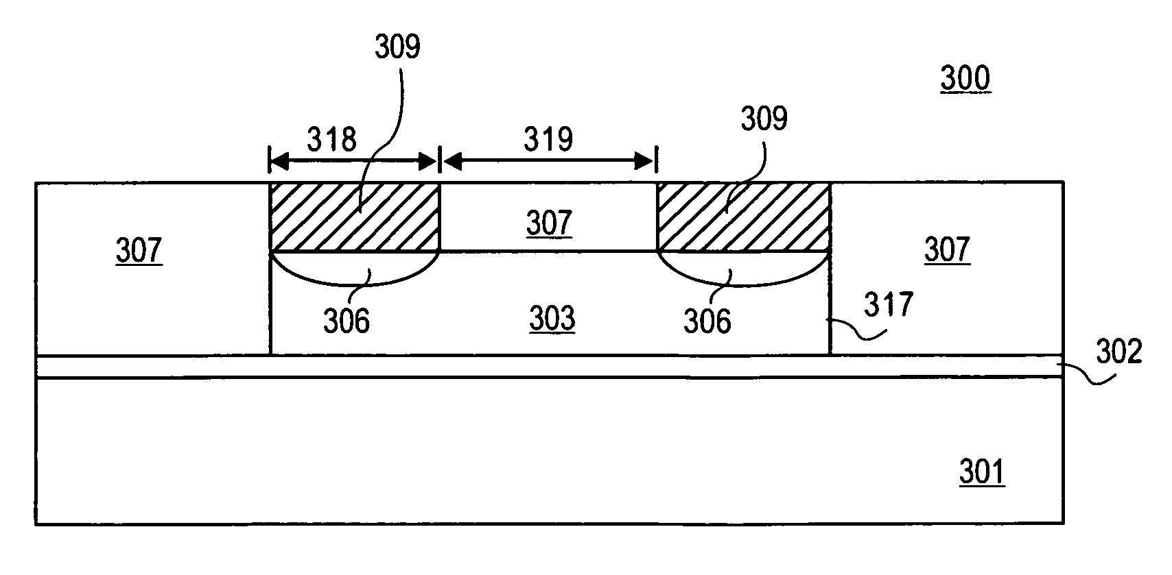
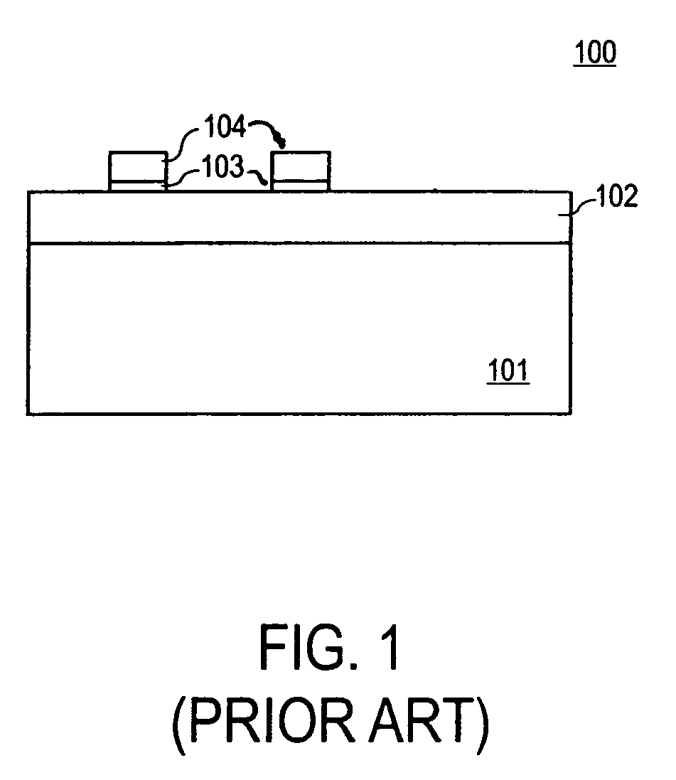
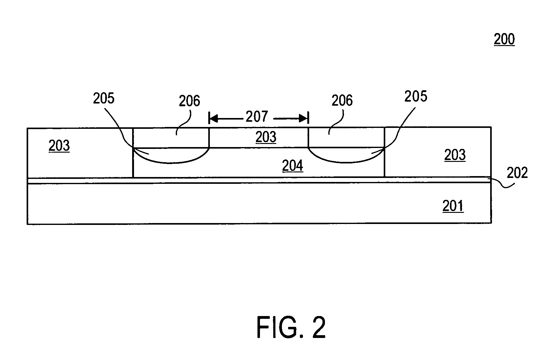
[0019]In the following description, numerous specific details, such as specific materials, dimensions of the elements, chemical names, etc. are set forth in order to provide thorough understanding of one or more of the embodiments of the present invention. It will be apparent, however, to one of ordinary skill in the art that the one or more embodiments of the present invention may be practiced without these specific details. In other instances, semiconductor fabrication processes, techniques, materials, equipment, etc., have not been described in great details to avoid unnecessarily obscuring of this description. Those of ordinary skill in the art, with the included description, will be able to implement appropriate functionality without undue experimentation.

[0020]While certain exemplary embodiments of the invention are described and shown in the accompanying drawings, it is to be understood that such embodiments are merely illustrative and not restrictive of the current invention...


PUM


Abstract

Metal-Semiconductor-Metal (“MSM”) photodetectors and methods to fabricate thereof are described. The MSM photodetector includes a thin heavily doped (“delta doped”) layer deposited at an interface between metal contacts and a semiconductor layer to reduce a dark current of the MSM photodetector. In one embodiment, the semiconductor layer is an intrinsic semiconductor layer. In one embodiment, the thickness of the delta doped layer is less than 100 nanometers. In one embodiment, the delta doped layer has a dopant concentration of at least 1×1018 cm−3. A delta doped layer is formed on portions of a semiconductor layer over a substrate. Metal contacts are formed on the delta doped layer. A buffer layer may be formed between the substrate and the semiconductor layer. In one embodiment, the substrate includes silicon, and the semiconductor layer includes germanium.

Description

FIELD[0001]Embodiments of the invention relate generally to the field of semiconductor manufacturing, and more specifically, to semiconductor photodetectors and methods to fabricate thereof.BACKGROUND[0002]Currently, dimensions of integrated circuits continue to be scaled down while signal frequencies continue to increase. Scaling down the dimensions of integrated circuits and higher frequencies may put limitations on use of the electrical interconnects, especially for the longer global interconnects. On-chip optical interconnects have the potential to overcome limitations of the electrical interconnects, especially limitations of the global electrical interconnects. A typical optical interconnect link includes a photodetector. Two of the critical parameters of the photodetector are the dark current and the signal-to-noise ratio (“SNR”). The dark current is generally defined as a current that flows in the photodetector when there is no optical radiation incident on the photodetector...

Claims


Application Information

Patent Timeline
IPC IPC(8): H01L29/739H01L27/095H01L29/47H01L29/80H01L29/812H01L31/00H01L31/0328H01L31/0336H01L31/07H01L31/072H01L31/109H01L31/112
CPCH01L31/1085H01L31/022408
Inventor RAKSHIT, TITASHRESHOTKO, MIRIAM
Owner INTEL CORP
Why Eureka
Try Eureka