Methods of fabricating delta doped silicon carbide metal-semiconductor field effect transistors having a gate disposed in a double recess structure

a technology of metal-semiconductor field effect transistor and delta-doped silicon carbide, which is applied in the direction of transistors, semiconductor devices, electrical equipment, etc., can solve the problems of limited power handling capability of previously known jfets, large heat generation of high-power and high-frequency transistors, and limited power handling capability of such devices at higher operating frequencies

Inactive Publication Date: 2005-06-07
CREE INC
View PDF55 Cites 22 Cited by
  • Summary
  • Abstract
  • Description
  • Claims
  • Application Information

AI Technical Summary

Benefits of technology

[0054]As is briefly described above, MESFETs according to embodiments of the present invention provide a double recessed gate structure which may simultaneously increase breakdown voltage and reduce source and drain resistances relative to conventional MESFETs. This may provide an advantage over conventional field effect transistors utilizing delta doped layers that sacrifice source and drain resistance to obtain a high breakdown voltage.

Problems solved by technology

Previously, bipolar transistors and power metal-oxide semiconductor field effect transistors (MOSFETs) have been used for high power applications but the power handling capability of such devices may be limited at higher operating frequencies.
Junction field-effect transistors (JFETs) were commonly used for high frequency applications but the power handling capability of previously known JFETs may also be limited.
In turn, high power and high frequency transistors usually generate larger amounts of heat than small signal transistors.
Although these devices provided increased operating frequencies and moderately increased power handling capability, the relatively low breakdown voltage and the lower thermal conductivity of these materials have limited their usefulness in high power applications.
Unfortunately, difficulty in manufacturing has limited the usefulness of SiC for high power and high frequency applications.
Although the SiC on Si substrate devices described in U.S. Pat. Nos. 4,762,806 and 4,757,028 may have exhibited improved thermal characteristics, the use of a Si substrate generally limits the ability of such devices to dissipate heat.
Furthermore, the growth of SiC on Si generally results in defects in the epitaxial layers which result in high leakage current when the device is in operation.
However, these devices also have increased source and drain resistances due to the lower mobility of the delta doped channel, which is not desirable.

Method used


Image

  • Methods of fabricating delta doped silicon carbide metal-semiconductor field effect transistors having a gate disposed in a double recess structure
  • Methods of fabricating delta doped silicon carbide metal-semiconductor field effect transistors having a gate disposed in a double recess structure
  • Methods of fabricating delta doped silicon carbide metal-semiconductor field effect transistors having a gate disposed in a double recess structure

Examples


Embodiment Construction

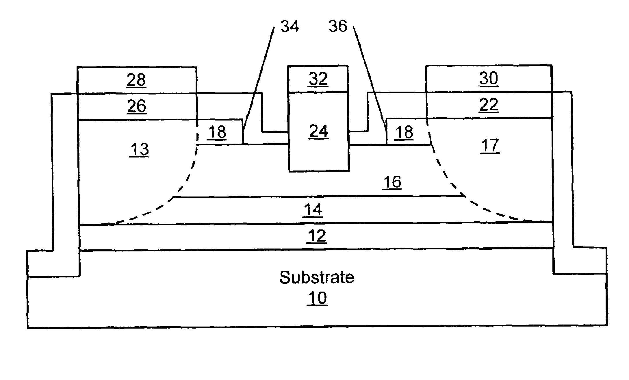
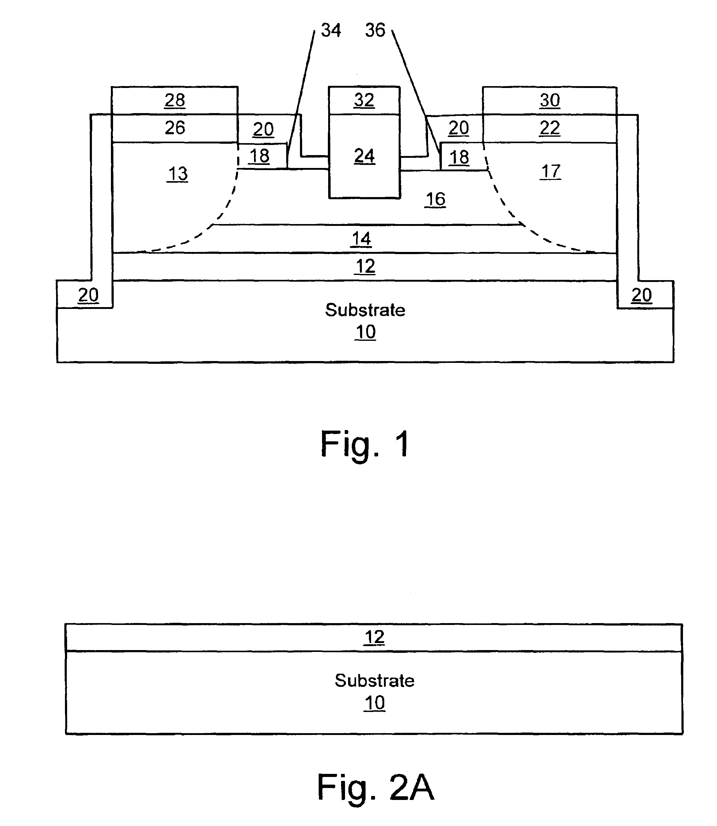
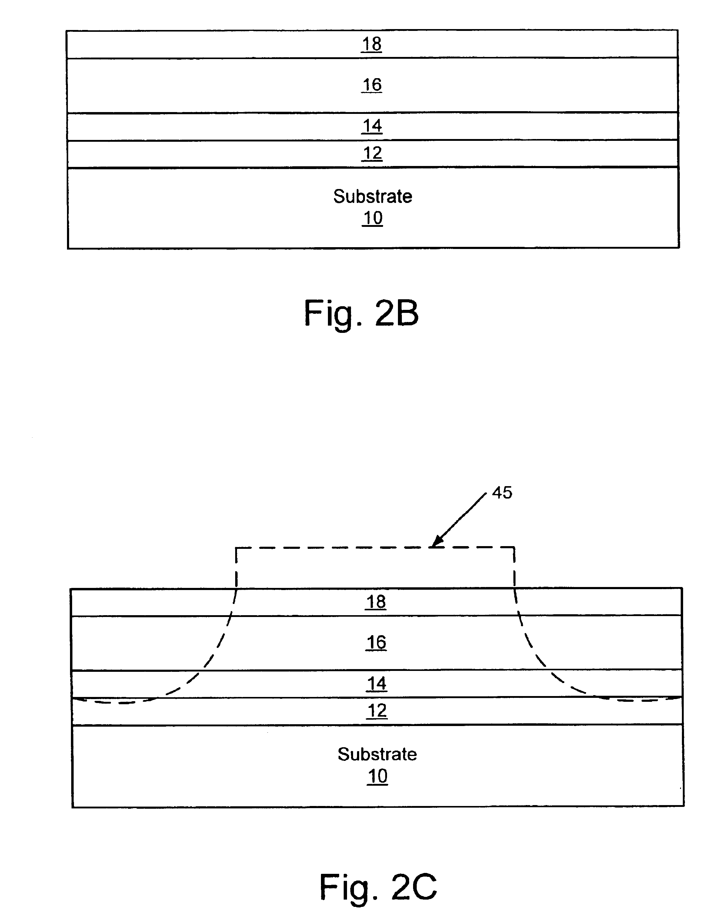
[0027]The present invention will now be described with reference to the FIGS. 1 and 2A-2H which illustrate various embodiments of the present invention. As illustrated in the Figures, the sizes of layers or regions are exaggerated for illustrative purposes and, thus, are provided to illustrate the general structures of the present invention. Furthermore, various aspects of the present invention are described with reference to a layer being formed on a substrate or other layer. As will be appreciated by those of skill in the art, references to a layer being formed on another layer or substrate contemplates that additional layers may intervene. References to a layer being formed on another layer or substrate without an intervening layer are described herein as being formed “directly” on the layer or substrate. Like numbers refer to like elements throughout.

[0028]Embodiments of the present invention will now be described in detail below with reference to FIGS. 1 and 2A-2H which illustr...


PUM

PropertyMeasurementUnit
poweraaaaaaaaaa
saturated electron drift velocityaaaaaaaaaa
carrier concentrationaaaaaaaaaa

Abstract

The present invention provides a unit cell of a metal-semiconductor field-effect transistor (MESFET). The unit cell of the MESFET includes a delta doped silicon carbide MESFET having a source, a drain and a gate. The gate is situated between the source and the drain and extends into a doped channel layer of a first conductivity type. Regions of silicon carbide adjacent to the source and the drain extend between the source and the gate and the drain and the gate, respectively. The regions of silicon carbide have carrier concentrations that are greater than a carrier concentration of the doped channel layer and are spaced apart from the gate.

Description

RELATED APPLICATION[0001]The present application is a divisional of and claims priority from co-pending U.S. application Ser. No. 10 / 136,456, filed Oct. 24, 2001, entitled “DELTA DOPED SILICON CARBIDE METAL-SEMICONDUCTOR FIELD EFFECT TRANSISTORS HAVING A GATE DISPOSED IN A DOUBLE RECESS STRUCTURE,” which is assigned to the assignee of the present application, the disclosure of which is hereby incorporated herein by reference as if set forth fully.FIELD OF THE INVENTION[0002]The present invention relates to microelectronic devices and more particularly to metal-semiconductor field-effect transistors (MESFETs) formed in silicon carbide.BACKGROUND OF THE INVENTION[0003]Electrical circuits requiring high power handling capability (>20 watts) while operating at high frequencies such as radio frequencies (500 MHz), S-band (3 GHz) and X-band (10 GHz) have in recent years become more prevalent. Because of the increase in high power, high frequency circuits there has been a corresponding ...

Claims


Application Information

Patent Timeline
Patent Type & Authority Patents(United States)
IPC IPC(8): H01L29/66H01L29/812H01L29/24H01L29/02H01L29/36H01L21/28H01L21/338H01L27/095
CPCH01L29/8128H01L29/242H01L29/365H01L29/772
Inventor SRIRAM, SAPTHARISHI
Owner CREE INC
Why Eureka
Try Eureka