Optical element, method for manufacturing optical element and semiconductor laser device using the optical element

a manufacturing method and optical element technology, applied in the field of optical elements, can solve problems such as complex processing, and achieve the effect of increasing large the difference of refractive index

Inactive Publication Date: 2009-05-26
CANON KK
View PDF5 Cites 20 Cited by
  • Summary
  • Abstract
  • Description
  • Claims
  • Application Information

AI Technical Summary

Benefits of technology

[0026]oxidizing a part of the first layer located in a lower part of the pores to increase a difference of refractive indices between the first layer and the second layer.
[0027]The present invention can realize an optical element which can reliably acquire a difference of refractive indices between a member under a photonic crystal layer and the crystal layer without using such a stacking technique as in conventional processes; a method for manufacturing the optical element; and a semiconductor laser device with the use of the optical element.
[0028]In other words, the present invention can form a slab-type photonic crystal with a large difference of refractive index even in a semiconductor optical element having a plurality of layers with different compositions, in an easy process; and also can provide a slab-type two-dimensional photonic crystal element which can be applied not only to a passive element but also to an active element such as a laser.

Problems solved by technology

The high grade of the process technology is required specifically because a necessary layer in the stacking step needs to be removed afterwards because the layer is unnecessary for the element, and one epitaxial substrate alone cannot realize the element, which make the process complicated.

Method used


Image

  • Optical element, method for manufacturing optical element and semiconductor laser device using the optical element
  • Optical element, method for manufacturing optical element and semiconductor laser device using the optical element
  • Optical element, method for manufacturing optical element and semiconductor laser device using the optical element

Examples


embodiments

[0047]In the next place, examples according to the present invention will be described.

example 1

[0048]In Example 1, a slab-type two-dimensional photonic crystal element configured by applying the present invention will be described.

[0049]In the present example, a slab-type photonic crystal was formed on a GaAs substrate, which includes a selectively oxidized layer of an AlGaAs layer (containing 90% or more Al) used as a clad, and an AlGaAs layer (containing 70% or less Al) used as a core.

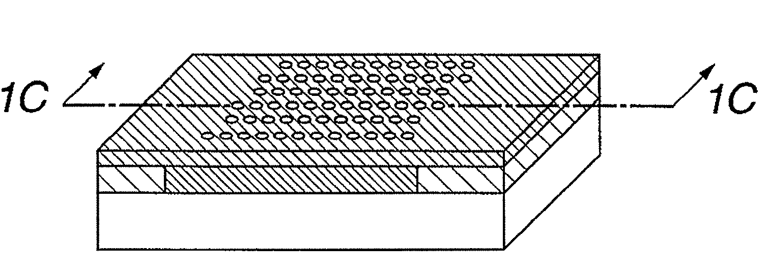
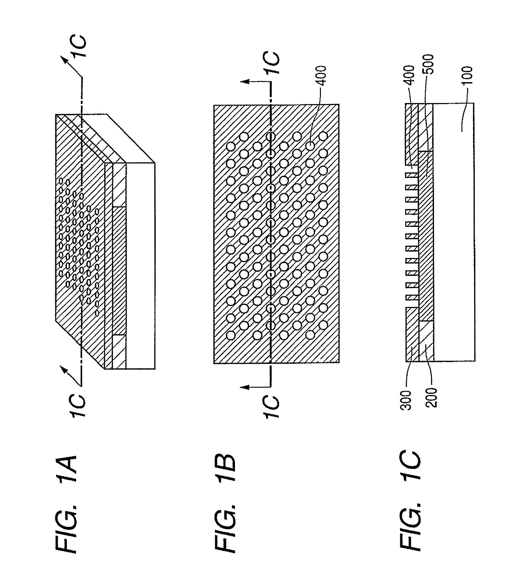
[0050]FIGS. 1A to 1C illustrate a configuration of the slab-type two-dimensional photonic crystal element according to the present example.

[0051]In FIGS. 1A to 1C, reference numeral 100 denotes the GaAs substrate, reference numeral 200 denotes the Al0.93Ga0.07As layer, reference numeral 300 denotes the Al0.5Ga0.5As layer, reference numeral 400 denotes a cylindrical hole and reference numeral 500 denotes an aluminum oxide layer.

[0052]As is illustrated in FIGS. 1A to 1C, a slab-type two-dimensional photonic crystal element produced in the present example includes a GaAs substrate 100; an Al0.93G...

example 2

[0069]In Example 2, a surface emitting laser will be described which employs a slab-type two-dimensional photonic crystal element according to the present invention.

[0070]FIG. 4 illustrates a configuration of the above described surface emitting laser according to the present example.

[0071]In FIG. 4, reference numeral 100 denotes a GaAs substrate, reference numeral 920 denotes an n-type Al0.93Ga0.07As / Al0.5Ga0.5As-DBR mirror layer, and reference numeral 1020 denotes an n-type AlGaInP clad layer.

[0072]In addition, reference numeral 1100 denotes a GaInP / AlGaInP multiquantum well active layer, reference numeral 1010 denotes a p-type AlGaInP clad layer and reference numeral 210 denotes a p-type Al0.93Ga0.07As layer.

[0073]Furthermore, reference numeral 310 denotes a p-type Al0.5Ga0.5As layer, reference numeral 400 denotes a cylindrical hole, reference numeral 500 denotes an aluminum oxide layer, reference numeral 1200 denotes a silicon nitride layer, reference numeral 1300 denotes an ano...


PUM


Abstract

The present invention provides an optical element which can reliably acquire a difference of refractive indices between a member under a photonic crystal layer and the crystal layer without using such a stacking technique as in conventional processes; a method for manufacturing the optical element; and a semiconductor laser device with the use of the optical element. The optical element has the first layer 500 and the second layer 400 formed on a substrate 100, wherein the second layer includes pores and has a refractive-index periodically changing structure in which a refractive index periodically changes in an in-plane direction; and the first layer has an oxidized region with a lower refractive index than the refractive index of the second layer, in a lower side of the pores of the second layer.

Description

BACKGROUND OF THE INVENTION[0001]1. Field of the Invention[0002]The present invention relates to an optical element, a method for manufacturing the optical element and a semiconductor laser device using the optical element.[0003]2. Description of the Related Art[0004]In recent years, research on a photonic crystal has been actively conducted.[0005]The photonic crystal means a structure which is formed of substances periodically repeating different refractive indices, and thereby causes a wavelength range (photonic band gap) in which light is inhibited from propagating, similarly to a band gap existing in an electronic state of a crystal.[0006]By using the photonic crystal, it becomes possible to two-dimensionally or three-dimensionally confine light in the crystal, so that the photonic crystal is tried to be applied to an optical waveguide or a mirror for a semiconductor laser.[0007]Technologies with the use of various techniques have been proposed in order to produce the two-dimens...

Claims


Application Information

Patent Timeline
Patent Type & Authority Patents(United States)
IPC IPC(8): H01S5/00
CPCB82Y20/00G02B6/1225H01S5/18311H01S5/0655H01S5/105H01S5/2081H01S5/3211H01S5/34326H01S5/3436H01S2301/166H01S5/11
Inventor UCHIDA, TATSURO
Owner CANON KK
Why Eureka
Try Eureka