Spatial light modulator featured with an anti-reflective structure

a technology of anti-reflective structure and spatial light, applied in the field of image display apparatus, can solve the problems of limited image display quality, adverse effects on image quality, and limited image quality, and achieve the effect of preventing a degradation of image contras

Inactive Publication Date: 2009-06-02
IGNITE INC
View PDF3 Cites 20 Cited by
  • Summary
  • Abstract
  • Description
  • Claims
  • Application Information

AI Technical Summary

Benefits of technology

[0039]One aspect of the present invention is to provide a spatial light modulator (SLM) having a mirror surface formed with a cyclic structure which is shorter than a wavelength of an incident light for reducing a reflecting light other than the modulating portion of a light reflected from the SLM and a package for accommodating the spatial light modulator.
[0040]Another aspect of the present invention is to provide a spatial light modulator (SLM) or a package for a spatial light modulator (SLM) with an anti-reflective structure. Also, the present invention discloses an image display apparatus that implements the antireflective structure both on the SLM and on the package to prevent unnecessary light reflection such that the display quality is improved with better contrast because the interferences from the unnecessary reflecting light is reduced.
[0044]The aspects of the present invention noted above make it possible to prevent a degradation of the contrast of an image caused by the unnecessary reflection light.

Problems solved by technology

Even though there are significant advances of the technologies implementing an electromechanical mirror device as a spatial light modulator (SLM) in recent years, there are still limitations and difficulties when it is employed to provide a high quality image.
Specifically, when the images are digitally controlled, the image quality is adversely affected due to the fact that the images are not displayed with sufficient number of gray scales.
The quality of an image display is limited due to the limited number of gray scales.
Since the mirror is controlled to operate in an either ON or OFF state, the conventional image display apparatuses have no way to provide a pulse width to control the mirror that is shorter than the control duration allowable according to the LSB.
The limited gray scale leads to a degradation of the image.
In this configuration, a reflected light that is not controlled for purposefully applied for image display is however inadvertently generated by reflections through the gap between adjacent mirrors.
As a result, a quality of the image display is worsened.
That leads to the degradations of image qualities.
The artifacts are caused by a technical limitation that the digitally controlled image does not obtain sufficient number of the gray scale, i.e. the levels of the quantity of light.
The mirrors produced by applying the CMOS technologies probably is not appropriate for operating the mirror at such a high range of voltages, and therefore the DMOS mirror devices may be required.
Conventional mirror controls are therefore faced with a technical problem that the good accuracy of gray scales and range of the operable voltage have to be sacrificed for the benefits of a smaller image display apparatus.
However, these patents or patent applications do not provide an effective solution to attain a sufficient number of the gray scale in the digitally controlled image display system.
However, these inventions do not provide a direct solution for a person skilled in the art to overcome the above-discussed limitations and difficulties.
As a result, the contrast of the image is degraded.
Also, the light arriving at a substrate from a gap between the adjacent light modulation elements is reflected on the substrate to become an unnecessary reflection light.
And the unnecessary reflection light entering the projection path decreases the contrast of an image.
This consequently is faced with the problem of increasing the number of producing processes.
On the other hand, a coating of a black material that is the simplest method for forming a light absorption layer is difficult to apply to a micro electro mechanical system (MEMS) device possessing a very minute structure.
As an example, there is a problem associated with the process for depositing a thin layer of carbon black in a specific place.

Method used


Image

  • Spatial light modulator featured with an anti-reflective structure
  • Spatial light modulator featured with an anti-reflective structure
  • Spatial light modulator featured with an anti-reflective structure

Examples


embodiment 1

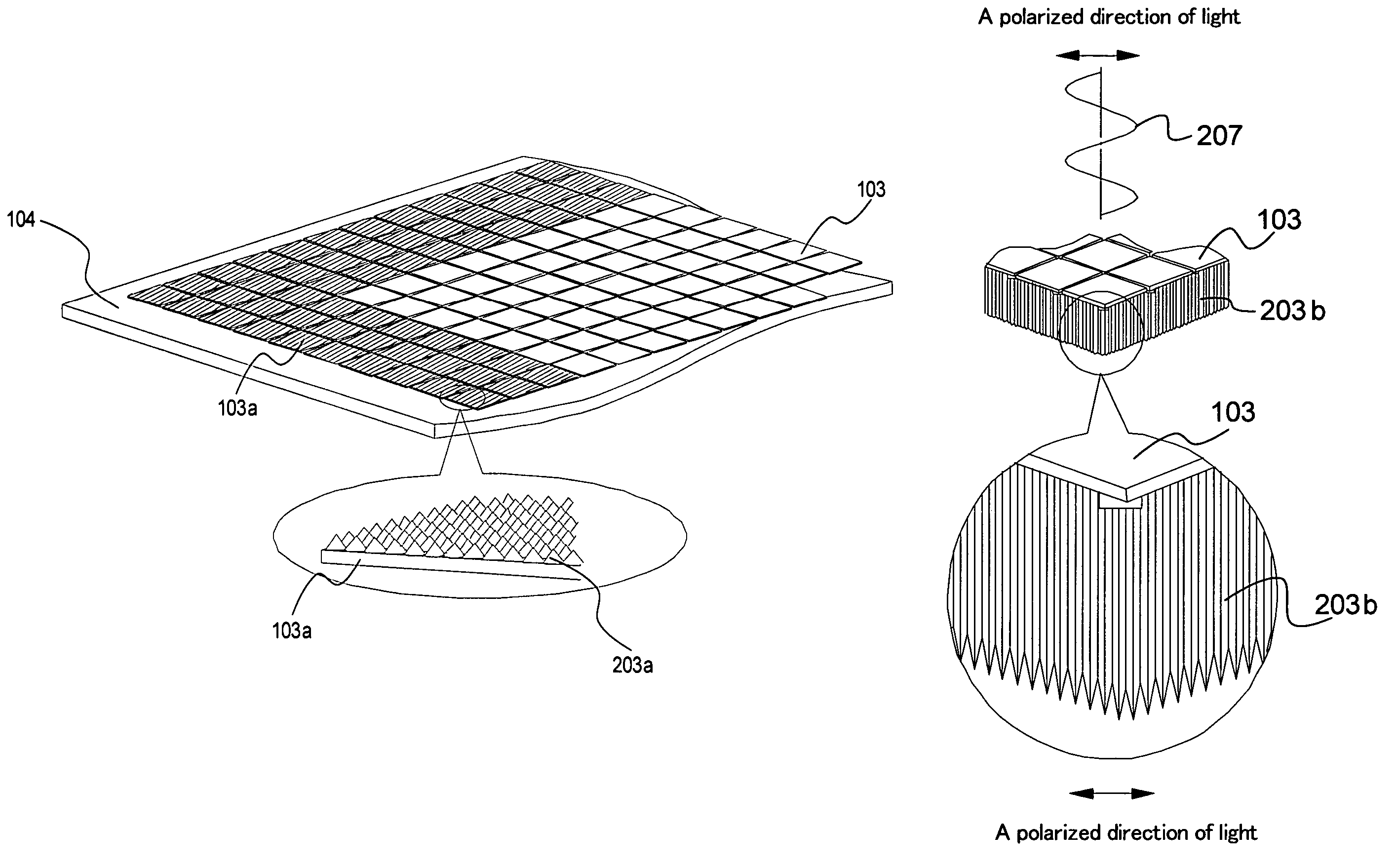
[0086]A mirror device includes an anti-reflection structure is disclosed as a preferred embodiment 1. FIG. 4 illustrates an exemplary mirror device that includes an anti-reflection structure formed on the device substrate. Specifically, FIG. 4 shows a front cross-section view of an assembly body 200a that function as a package for accommodating a mirror device. FIG. 4 shows only two mirror elements in the mirror device as an example. The assembly body 200a comprises a mirror device, a package substrate 201 and a cover member 202. The package actually includes other parts in additional to the mirror device. The package includes package substrate 201 and cover member 202 shown in FIG. 4 and these parts are part of the package.

[0087]Further details for the constituent component of the assembly body 200a are described below according what are shown in FIG. 4. It is understood that the term “inside of the package” noted in the present specification refers to a space sealing a mirror devi...

embodiment 2

[0092]The following descriptions are for a package featured with an anti-reflection structure as an embodiment 2. The embodiment 2 is a modified example of the embodiment 1. The package according to the embodiment 2 is configured to feature an anti-reflection structure on the internal and external wall surfaces of the package substrate of the embodiment 1. Other configuration of the embodiment 2 is similar to that of the embodiment 1 and therefore the description is omitted here.

[0093]FIG. 5A is a front cross-section diagram of an assembly body 200b-I featured with an anti-reflection structure on the internal wall of the package substrate 201 of the embodiment 1. The assembly body 200b-I shown in FIG. 5A is featured with the anti-reflection structure described above on the inner wall on the package substrate 201b-I. A light reflected on the mirror 103 is prevented from being further reflected on the inner wall of the package substrate 201b-I by the anti-reflection structure featured...

embodiment 3

[0097]The next is a description on a mirror featured with an anti-reflection structure, as an embodiment 3. The embodiment 3 is a modified example of the embodiment 1. The embodiment 3 is configured to feature an anti-reflection structure on the bottom surface of the mirror 103 of the embodiment 1. Other configurations of the embodiment 3 are similar to that of the embodiment 1 and therefore the description is omitted here.

[0098]FIG. 6 is a front cross-section diagram of an assembly body 200c featured with an anti-reflection structure on the bottom surface of the mirror 103 of the embodiment 1. The assembly body 200c shown in FIG. 6 is configured to feature an anti-reflection structure on the bottom surface of the mirror 103. Such a configuration makes it possible to prevent a light reflected on the edge of the mirror 103c from being further reflected on the bottom surface of the adjacent mirror 103c by the anti-reflection structure featured on the bottom surface of the adjacent mir...


PUM

PropertyMeasurementUnit
deflection angleaaaaaaaaaa
lengthaaaaaaaaaa
diagonal lengthaaaaaaaaaa

Abstract

A spatial light modulator supported on a device substrate includes a plurality of light modulation elements to modulate a light emitted from a light source. The spatial light modulator and the device substrate further comprises a cyclic structure on a surface of the spatial light modulator and / or the device substrate for preventing a reflection of the incident light from the cyclic structure. In an exemplary embodiment the cyclic structure includes cyclic structural elements having a distance between two cyclic elements shorter than the wavelength of an incident light for preventing a reflection of the incident light from the cyclic structure.

Description

CROSS REFERENCE TO RELATED APPLICATIONS[0001]This application is a Non-provisional application of a Provisional Application 60 / 830,171 filed on Jul. 12, 2006. The Provisional Application 60 / 830,171 is a Continuation In Part (CIP) Application of U.S. patent application Ser. No. 11 / 121,543 filed on May 4, 2005 now U.S Pat. No. 7,268,932. The application Ser. No. 11 / 121,543 is a Continuation In Part (CIP) application of three previously filed Applications. These three applications are Ser. No. 10 / 698,620 filed on Nov. 1, 2003, Ser. No. 10 / 699,140 filed on Nov. 1, 2003 now U.S. Pat. No. 6,862,127, and Ser. No. 10 / 699,143 filed on Nov. 1, 2003 now U.S. Pat. No. 6,903,860 by the Applicant of this patent applications. The disclosures made in these patent Applications are hereby incorporated by reference in this patent application.BACKGROUND OF THE INVENTION[0002]1. Field of the Invention[0003]The present invention relates to an image display system. More particularly, the present invention...

Claims


Application Information

Patent Timeline
Patent Type & Authority Patents(United States)
IPC IPC(8): G02B26/00G02B26/08G02F1/29
CPCG02B1/118G02B26/0833G02F1/136277H04N9/3141G02F2201/38G02F2203/12
Inventor ISHII, FUSAOMAEDA, YOSHIHIROICHIKAWA, HIROTOSHIWATANABE, KAZUHIROHORIKAWA, YOSHIAKI
Owner IGNITE INC
Why Eureka
Try Eureka