Structure for reducing stress for vias and fabricating method thereof

a stress block and stress reduction technology, applied in the direction of printed circuit stress/warp reduction, printed circuit aspects, printed circuit manufacturing, etc., can solve the problems of mismatched thermal stress in the interface area of different materials, difficulty in process and product reliability, etc., to achieve the effect of enduring stress and strain

Inactive Publication Date: 2009-06-09
IND TECH RES INST
View PDF3 Cites 0 Cited by
  • Summary
  • Abstract
  • Description
  • Claims
  • Application Information

AI Technical Summary

Benefits of technology

[0009]In view of the above problems, the object of the present invention is to provide a structure for reducing stress for vias and a fabricating method thereof, thereby to solve the problem of failing to effectively withstand the stress and strain resulting from the innate material disclosed in the prior art.
[0010]Therefore, in order to achieve the above object, the structure for reducing stress for vias disclosed in the present invention comprises an insulation layer, a stress block, a first conductor, a second conductor, and a via. The stress block is disposed in the insulation layer and is in a lattice structure. The first conductor and the second conductor are respectively disposed on the two sides of the insulation layer. The via passes through the interior of the stress block and run through the insulation layer to connect the first conductor and the second conductor. Thus, the shear stress generated by the insulation layer under temperature loading can be blocked or absorbed by the stress block, thereby protecting the via and thus improving the reliability of the via and electronic elements.

Problems solved by technology

Difficulties in the process and the reliability of products have increasingly emerged; therefore, in order to achieve a single die with high volume or a stacked packaging with multiple die, the requirements of high volume and high speed are reached by the use of different package structures.
Since there are generally various kinds of materials in different kinds of electronic devices or elements, the mismatched thermal stresses in the interface areas of different materials will be caused by the difference in the temperature distribution and the CTE of different materials.
Thus, the telecommunicating contact is destroyed, for example the breaking of the wire in the thickness direction, thereby causing problems with product reliability.
However, the physical characteristics subject to the material cannot be changed and the materials compatible with the process which can be selected for use are limited.
Considering the temperature cycling of the reliability, the wire in the thickness direction tends to endure large stress and dramatic deformation due to the large amount thermal expansion of the insulating material.
However, when the insulating material with a low E serves as a stress-buffering device, the stress buffering effect will be increased as the thickness of the insulating material is increased, whereas the ratio of depth to width of the wire in the thickness direction will be excessively large.
Therefore, the problem resulting from the innate material cannot be effectively alleviated even if the structure which is designed with enlarged wall thickness or blind vias filled with metal materials is employed.

Method used


Image

  • Structure for reducing stress for vias and fabricating method thereof
  • Structure for reducing stress for vias and fabricating method thereof
  • Structure for reducing stress for vias and fabricating method thereof

Examples


Embodiment Construction

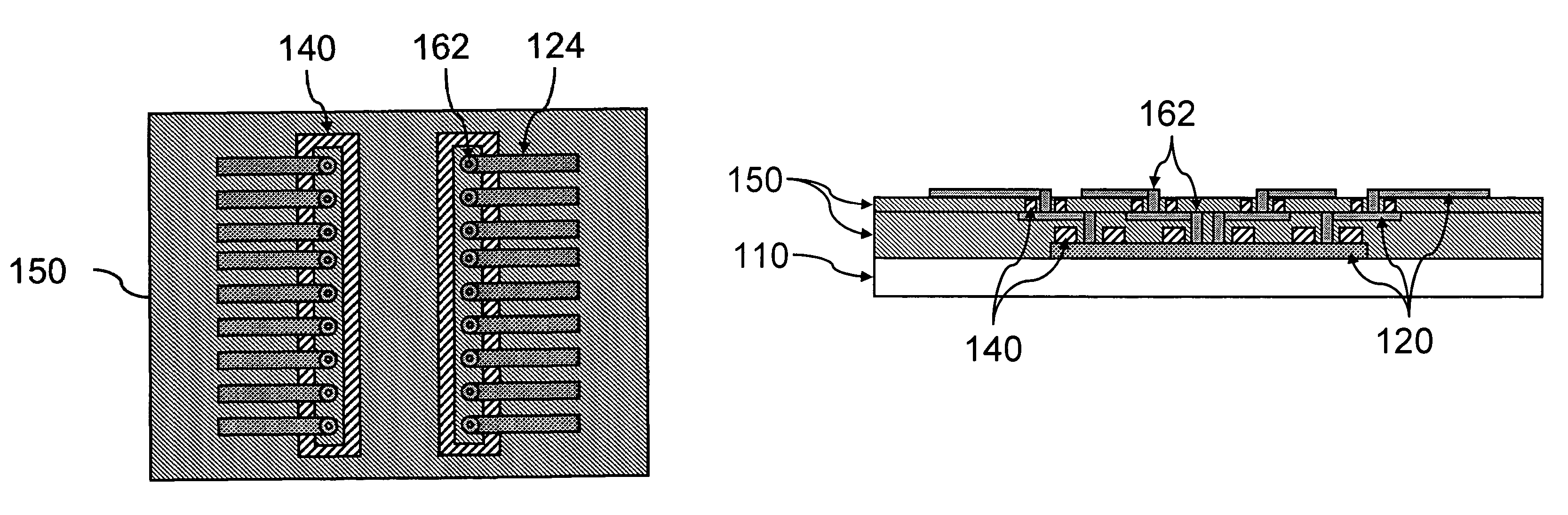
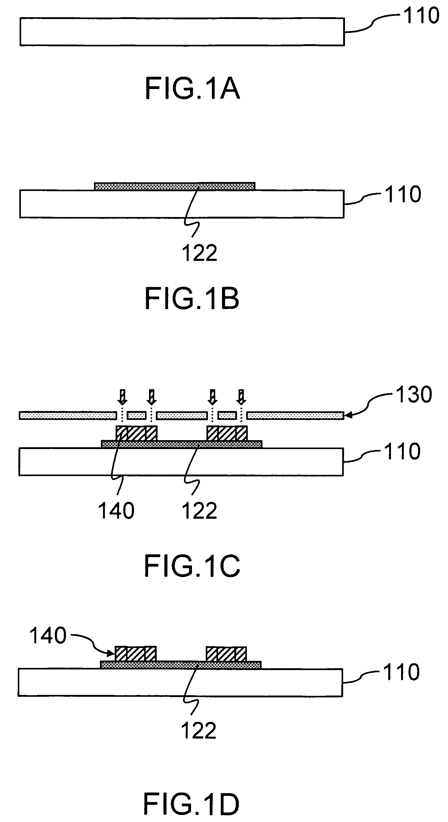
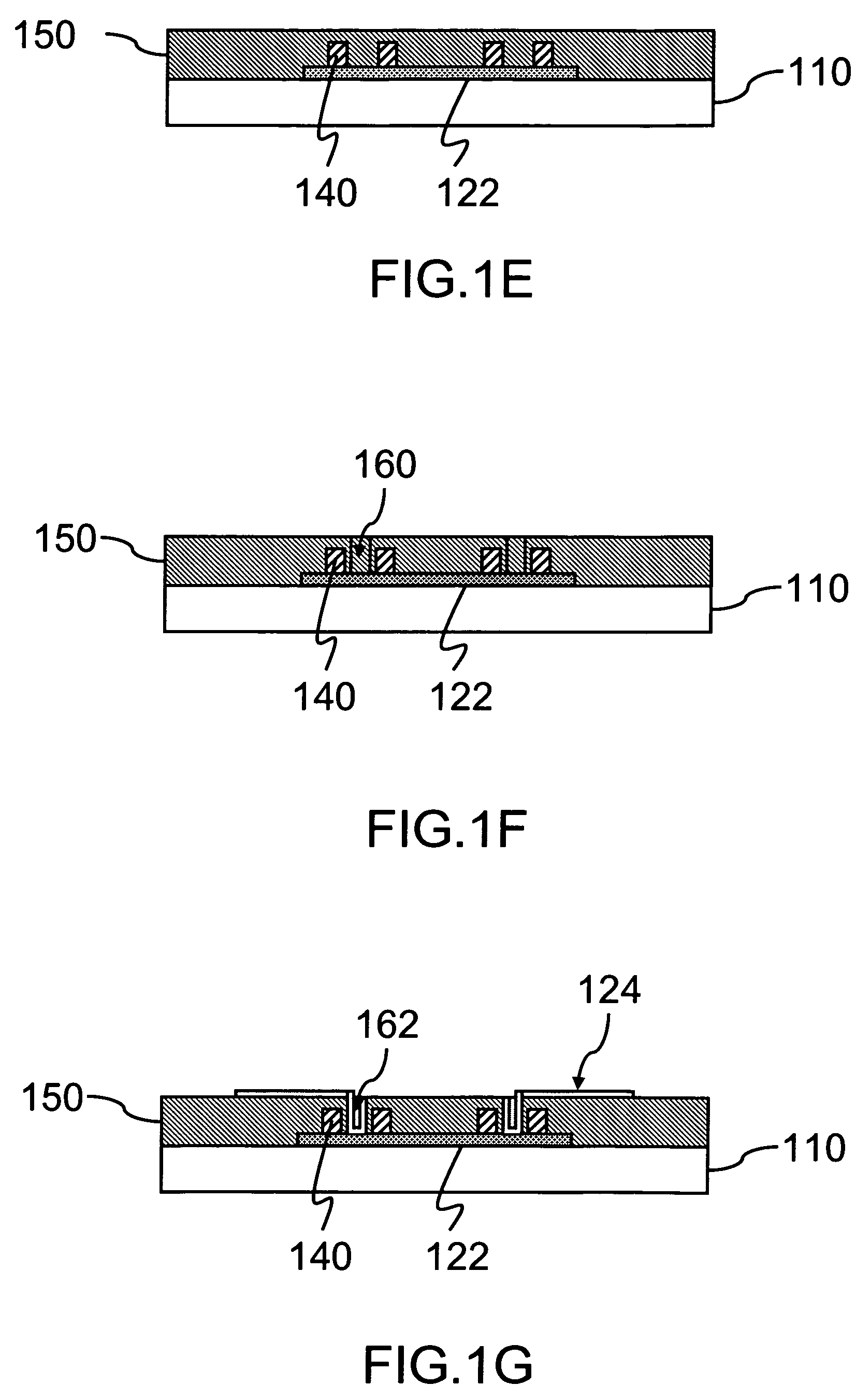
[0027]Herein, the method is mainly to enframe the wire in the thickness direction with a frame at the location adjacent to the wire structure (namely, via) in the thickness direction, so as to isolate the wire from contacting directly with the major portion of the material of a high CTE (Coefficient of Thermal Expansion). Therefore, the thermal expansion and the thermal stress resulted from different CTE of the materials of the electronic device or element can be “blocked” from the wire in the thickness direction within a fixed range, or be absorbed. Thus, the shear stress resulted from the CTE under temperature loading cannot have a direct effect on the wire in the thickness direction, thereby it is quite helpful in the long-time reliability required by the electronic devices or elements, regardless of the process, or the consumers. Therefore, the present invention can be extensively applied to various packaging structures such as Chip Size Package (CSP), Ball Grid Array (BGA) pack...


PUM


Abstract

A structure for reducing stress for vias and a fabricating method thereof are provided. One or more wires or vias in the thickness direction are enframed with the use of a stress block in a lattice structure to be isolated from being directly contacted with the major portion of insulating materials with a high coefficient of thermal expansion. Thus, the shear stress resulting from temperature loading can be blocked or absorbed by the stress block.

Description

CROSS-REFERENCE TO RELATED APPLICATIONS[0001]This non-provisional application claims priority under 35 U.S.C. § 119(a) on patent application Ser. No(s). 094140304 filed in Taiwan, R.O.C. on Nov. 16, 2005, the entire contents of which are hereby incorporated by reference.BACKGROUND OF THE INVENTION[0002]1. Field of Invention[0003]The invention relates to a stress block structure of an electronic packaging, and more particularly to a structure for reducing stress for vias and a fabricating method thereof.[0004]2. Related Art[0005]In recent years, as the demands of electronic products in speed and volume have increased dramatically, the amount of the input / output (I / O) pins and the power of the chips are increasing accordingly.[0006]Taking memory as an example, the volume of early memory was 16M or 64M. Now, memory has been developed to the Double Data Rate II Synchronous Dynamic Random Access Memory (DDRII SDRAM) with a volume of 512M. Difficulties in the process and the reliability o...

Claims


Application Information

Patent Timeline
Patent Type & Authority Patents(United States)
IPC IPC(8): H01L23/48H01L23/52H01L29/40
CPCH01L21/486H01L23/49827H01L23/562H01L24/19H05K1/0271H05K1/115H01L2224/04105H01L2224/20H01L2224/211H01L2924/01029H01L2924/01078H01L2924/01079H01L2924/12044H01L2924/15311H01L2924/3025H05K3/4644H05K2201/068H05K2201/09509H05K2201/09563H05K2201/09781H05K2201/09909H01L2924/01006H01L2924/01033H01L2224/12105H01L2924/351H01L2924/00
Inventor HSU, YUNG-YUFENG, RONG-CHANGTAIN, RA-MINLIAU, SHYI-CHINGLIN, JI-CHENGYU, SHAN-PUCHEN, SHOU-LUNGCHENG, CHIH-YUAH
Owner IND TECH RES INST
Why Eureka
Try Eureka