
Method of and apparatus for digital image processing

Inactive Publication Date: 2009-06-23
HEWLETT PACKARD DEV CO LP
View PDF10 Cites 8 Cited by
  • Summary
  • Abstract
  • Description
  • Claims
  • Application Information

AI Technical Summary

Benefits of technology

[0024]The present invention is in contrast to the arrangement described in International Patent Application No. WO99 / 62245, which employs a technique that relies upon interlacing and specifically avoids selecting sets of pixels for display from localised groups of pixels within the imaging matrix. In the present invention, the colour information required for the pixels of the viewfinder is derived from adjacent sensor pixels in order to minimise the effects of colour aliasing due to colour values being selected from separate parts of a focused image.
[0025]The present invention has the significant advantage of requiring minimal processing, and pixels can be selected for inclusion in a set of pixels for display or disregarded by, for example, a simple sequencer, without introducing any significant latency.
[0026]Disregarding pixels also reduces the bandwidth required to transmit pixel data from an image sensor of a camera to the display screen (which may be in the form of a viewfinder) and reduces any buffering requirement during transmission. A simple algorithm can be used to define the pattern of sets of pixels to be selected for display, and the pattern of selected sets can be defined to convert any image resolution to any lower display resolution. In one embodiment of the invention, the pattern can be redefined dynamically during image capture, so as to facilitate, for example, panning and zooming effects with minimum steps / displacements determined by the full resolution pixel pitch. It will be appreciated that the combination of pixels in a set produces a display pixel in full colour, thereby eliminating the need to demosaic the captured image data.
[0027]In general, the present invention provides a relatively cheap and flexible solution to the problem of generating a low-resolution viewfinder while also avoiding contributing significantly to viewfinder latency or power-consumption. It can be implemented in stand-alone cameras as well as embedded cameras and accessory cameras for use with PC-like devices.

Problems solved by technology

As technology advances, the resolution of modem cameras is increasing and the screen on which images are required to be displayed is often necessarily relatively small and has a comparatively low resolution.
Further, in many cases, the computation required to receive all of the image data representing a captured image, demosaic the image data (i.e. perform interpolation of all three base colours, namely red, green and blue or cyan, magenta and yellow for each pixel of an image) and reduce it so that the image fits the screen on which it is required to be displayed is too great to be able to effectively provide the viewfinder function referred to above without introducing an unacceptable level of displayed image latency, additional cost and / or greater power consumption.
However, this solution increases the cost and complexity of the image sensor and, in any event, does not solve the problems outlined above unless the reduced resolution image produced by the sensor matches the viewfinder display resolution for a particular device.
However, the use of the additional pre-processing chip can reduce the battery life of a portable device (because of its significant power consumption) and, in any event, substantially increases the overall product cost, which is clearly undesirable.
In yet another prior solution, whereby the camera function is provided in a portable device such as a personal digital assistant (PDA), a software scaling function is applied to an image prior to display thereof This provides a relatively low-cost solution to the problems outlined above, but requires the reading and processing of large amounts of data which, unless the device has a powerful processor and fast data transfer, may introduce significant latency in the viewfinder.
As explained above, in view of the large number of pixels involved, it is not possible to display all pixels in the viewfinder during operation.
However, this technique specifically relies on interlacing and specifically avoids reading out information from localised groups of pixels, with the result that significant image data may be lost and the quality of the resultant displayed image is compromised.

Method used


Image

  • Method of and apparatus for digital image processing
  • Method of and apparatus for digital image processing
  • Method of and apparatus for digital image processing

Examples


Embodiment Construction

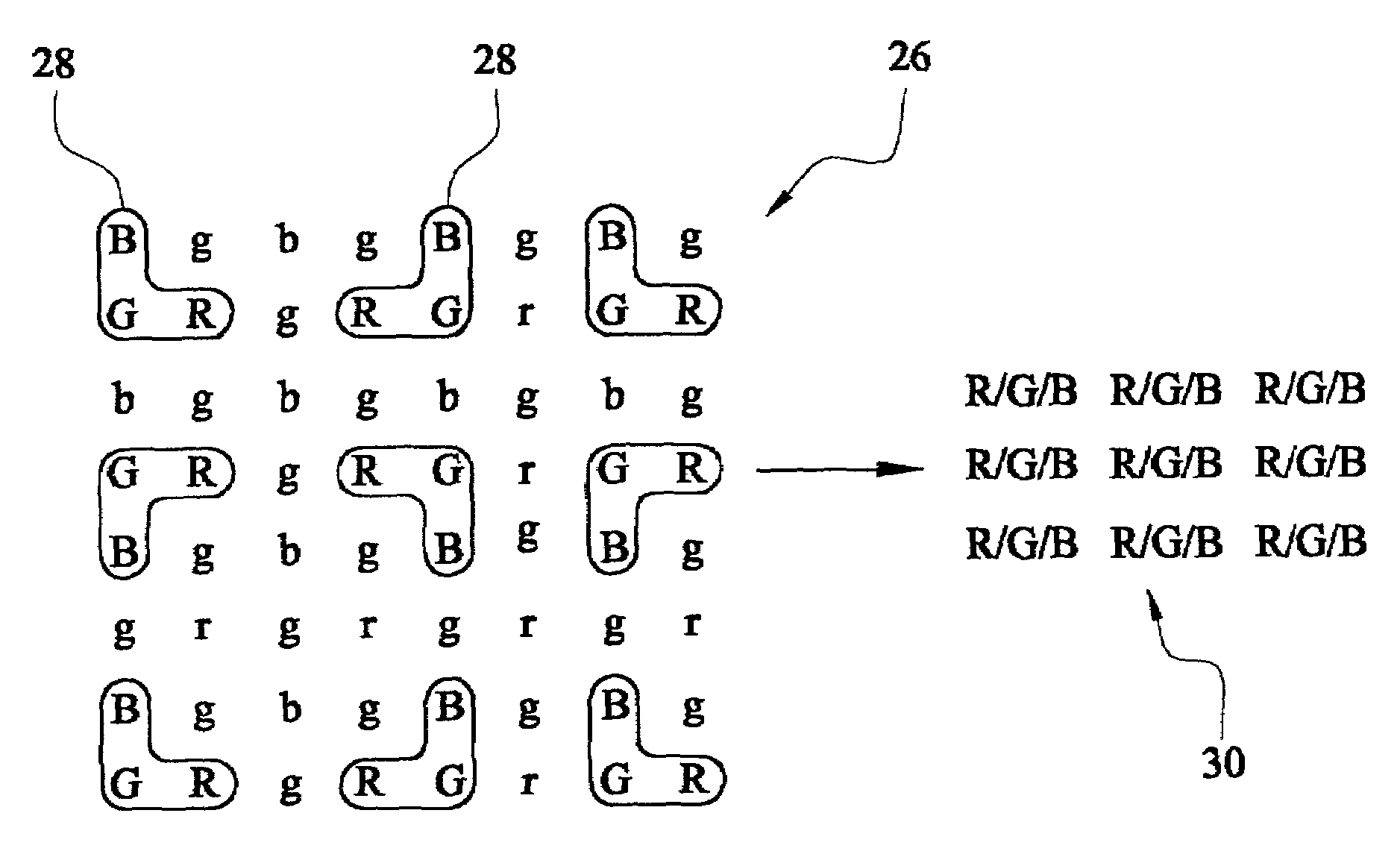
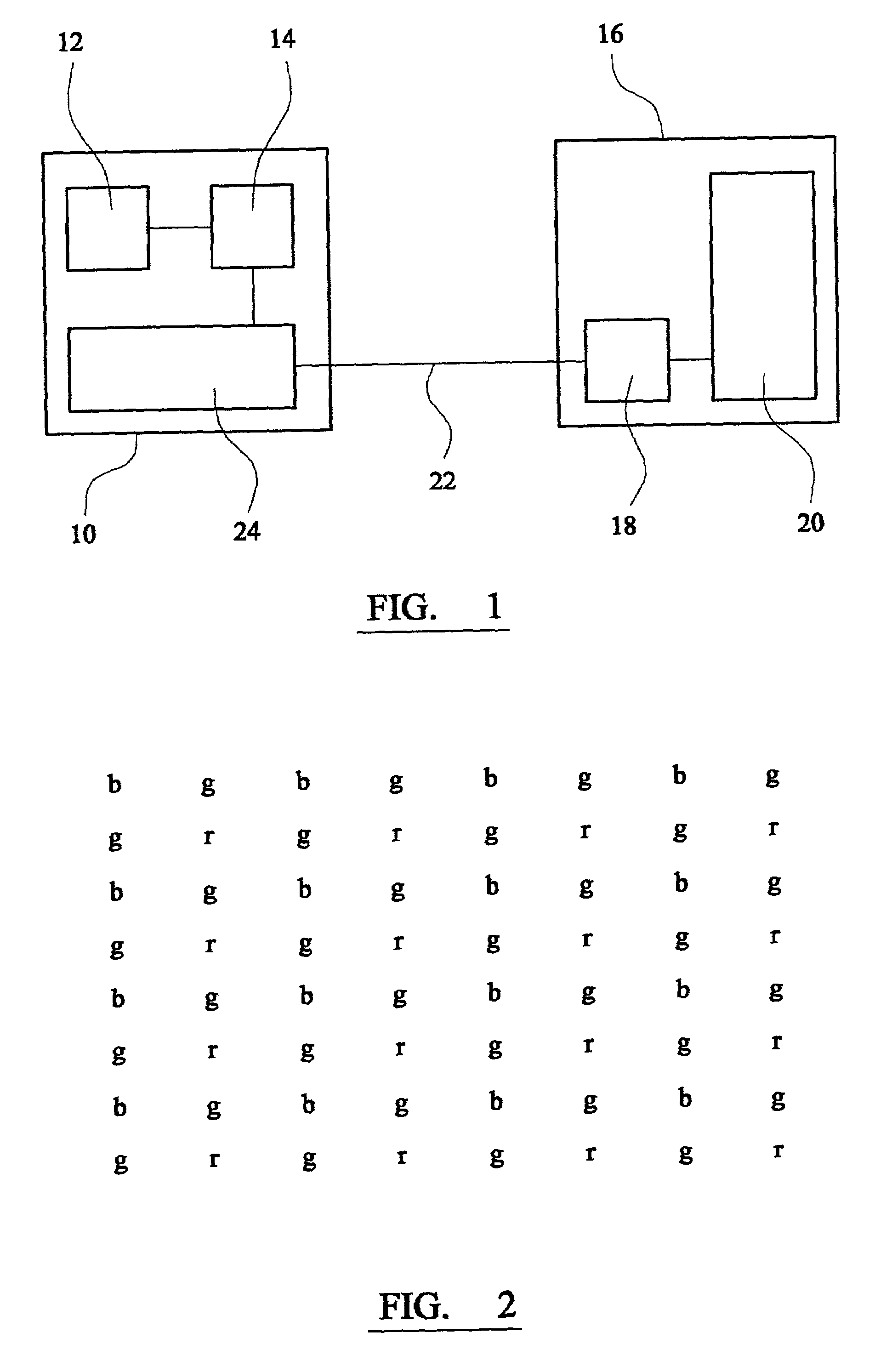
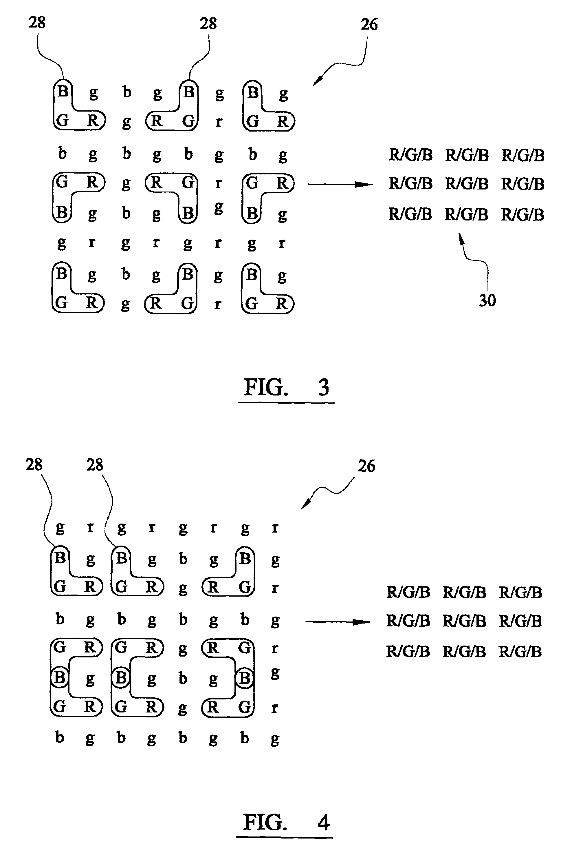
[0034]Referring to FIG. 1 of the drawings, apparatus according to an exemplary embodiment of the present invention comprises an image capture device 10 including an image sensor 12 for capturing image data, and an optional buffer memory 14 for storing captured data in the form of an imaging matrix. The sensor data consists of a sequence of red and green alternating pixels on one image row and a sequence of green and blue alternating pixels on the next row. This is known as a Bayer pattern, and is illustrated in FIG. 2 of the drawings.

[0035]The image sensor is preferably a CMOS image sensor. A CMOS image sensor is preferred in many prior art arrangements in view of the resultant ability to directly address rows and columns to avoid reading full image fields. However, in this exemplary embodiment of the present invention, this facility is specifically avoided, because by reading full images from the sensor it is possible to achieve better image quality and greater freedom to vary scal...


PUM


Abstract

An image incident on a pixel array having a Bayer pattern is compressed by grouping only some of the pixels in the Bayer pattern into sets including a triad of pixels of the Bayer pattern. The triad of pixels of each set includes the three primary colors and are next to each other in the rows, columns and diagonally within the Bayer pattern. The pixels in each set are combined to form a single pixel of the compressed array.

Description

FIELD OF THE INVENTION[0001]This invention relates to a method and apparatus for digital image processing and, more particularly, to a method and apparatus for processing digital images captured by one or more image capture devices prior to display thereof on a display screen.BACKGROUND TO THE INVENTION[0002]There are many circumstances in which it may be required to transmit image data captured by a camera to a host computer system for display thereby. For example, web cameras are well known which capture images and transmit image data to a remote host computer for display thereby. It is also common for a host device having camera functions to also have a display for viewfinding and for reviewing images captured by the camera.[0003]In general, the resolution of the display is substantially lower than the resolution of the images by the camera function. As technology advances, the resolution of modem cameras is increasing and the screen on which images are required to be displayed i...

Claims


Application Information

Patent Timeline
IPC IPC(8): G09G5/02G06T3/40
CPCG06T3/4015
Inventor HUNTER, ANDREW ARTHUR
Owner HEWLETT PACKARD DEV CO LP
Learn More