Method of manufacturing a printed wiring board having a previously formed opening hole in an innerlayer conductor circuit

a printing board and opening hole technology, applied in the direction of printed circuit non-printed electric components association, resistive material coating, etching metal masks, etc., can solve the problems of expensive control device for such adjustment, uneven depth accuracy, and inability to accurately adjust the intensity of laser beams, etc., to achieve easy and accurate formation, excellent heat dissipation, and high density wiring of printed wiring boards

Inactive Publication Date: 2009-06-30
IBIDEN CO LTD
View PDF52 Cites 17 Cited by
  • Summary
  • Abstract
  • Description
  • Claims
  • Application Information

AI Technical Summary

Benefits of technology

[0029]On the other hand, the irradiation of the laser beam is stopped at a time of reflecting on the innerlayer conductor circuit in the formation of the deep blind via-hole, so that damage is not caused.
[0208]As the inorganic filler added to the synthetic resin, there are glass fibers, silica powder, mica powder, alumina, carbon and the like. The substrate made of a mixture of the synthetic resin and the inorganic filler is higher in strength as compared with the synthetic resin alone.

Problems solved by technology

However, these drilling methods cause unevenness in the depth accuracy.
Therefore, it is complicated to adjust the intensity of the laser beam for every via-hole and also requires an expensive control device for such an adjustment.
Since the black oxide film is high in the energy absorption of laser beam, there is a fear of causing damages such as breakage and the like due to fusion and swelling of the innerlayer conductor circuit provided on its surface with the black oxide film.
Also, the insulating layer made of the resin or the like is exposed in the via-hole, so that it is difficult to form the metal plated film.
For this end, the joining property between the inner wall of the via-hole and the metal plated film is low resulting in peeling, dropping-out and the like of the metal plated film.
This can have a bad effect on the electric conduction of the via-hole.
However, as the inner diameter of the hole becomes small, it is difficult to make the formation of the plated film uniform, resulting in the electric conduction of the via-hole being insufficient.

Method used


Image

  • Method of manufacturing a printed wiring board having a previously formed opening hole in an innerlayer conductor circuit
  • Method of manufacturing a printed wiring board having a previously formed opening hole in an innerlayer conductor circuit
  • Method of manufacturing a printed wiring board having a previously formed opening hole in an innerlayer conductor circuit

Examples


embodiment 1

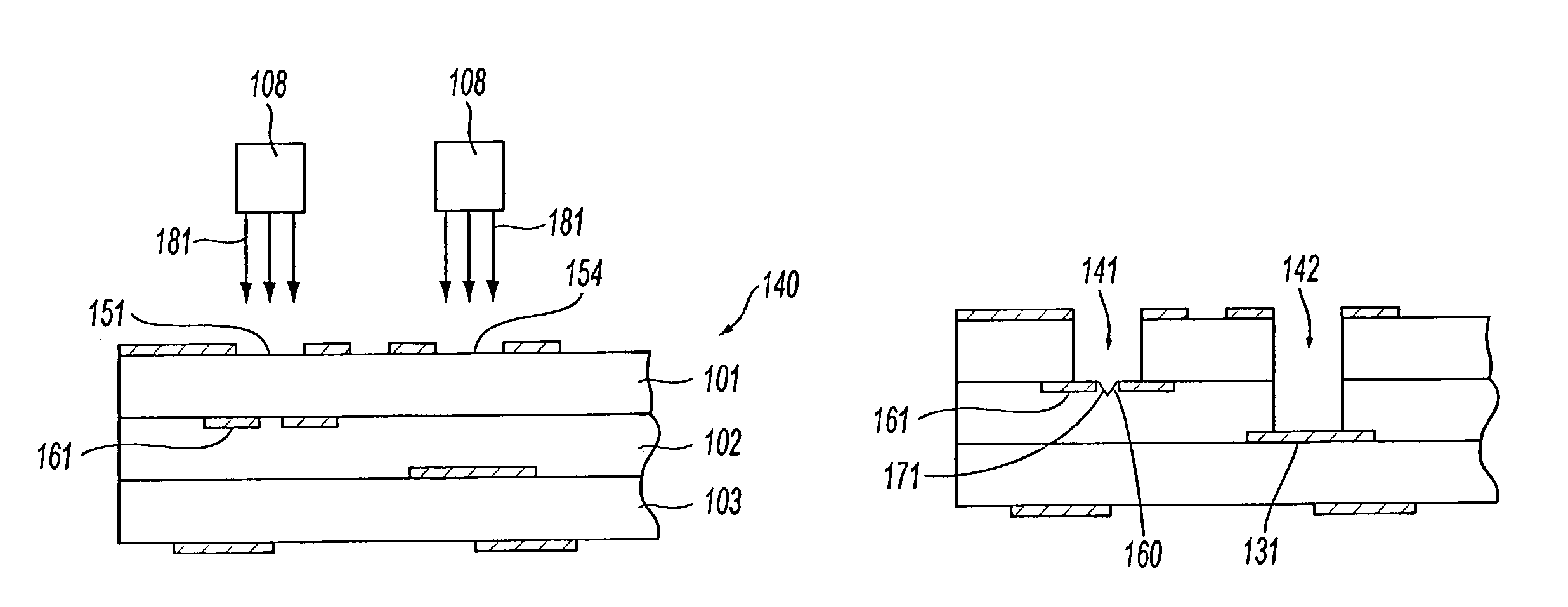
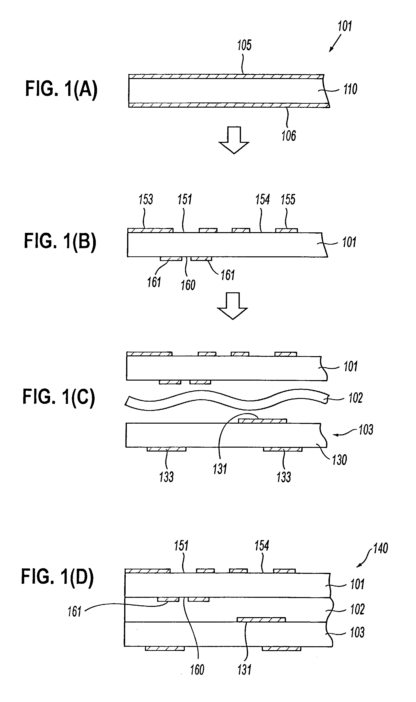
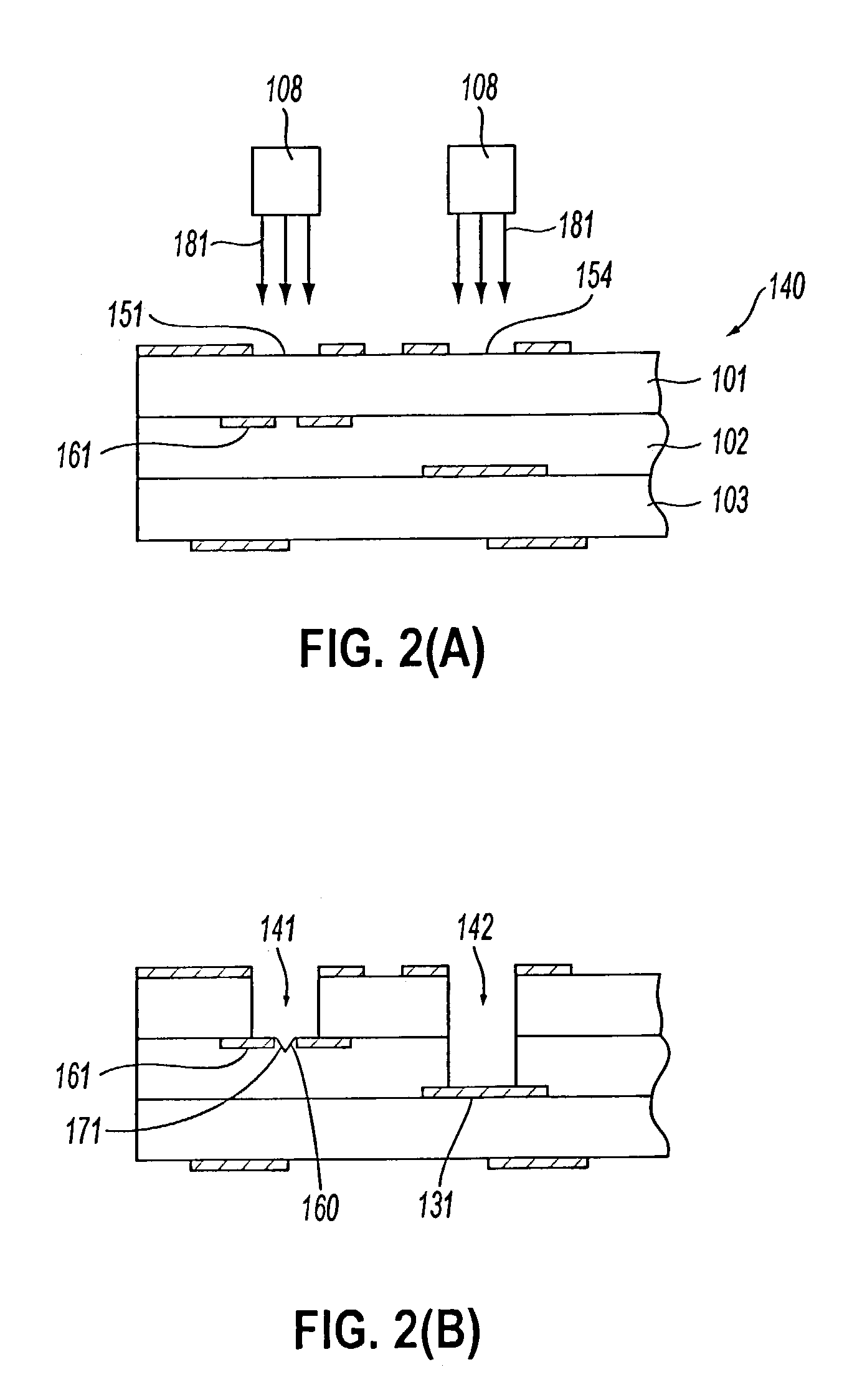
[0275]The production method of a first embodiment of the printed wiring board according to the first aspect of the invention is described with reference to FIG. 1 to FIG. 7.

[0276]At first, the printed wiring board to be produced in this embodiment comprises three insulating layers of a synthetic resin 101, 102, 103, innerlayer conductor circuits 161, 131 formed between these insulating layers 101-103 and blind via-holes 141, 142 formed from an outermost surface of the insulating layers 101-103 toward the innerlayer conductor circuits 161, 131 as shown in FIG. 6.

[0277]Also, metal plated films 175, 176 extending from the innerlayer conductor circuits 161, 131 to outer conductor circuits 153, 155 are formed on inner wall faces of the blind via-holes 141, 142. Moreover, an outer conductor circuit 133 is located at a lower face.

[0278]The production method of the above printed wiring board is described below.

[0279]As shown in FIG. 1(A), there is provided a first insulating layer 101. The ...

embodiment 2

[0297]The production method of a second embodiment of the printed wiring board according to the second aspect of the invention is described with reference to FIG. 8 to FIG. 10.

[0298]At first, the printed wiring board 210 to be produced in this embodiment comprises three insulating layers 211, 212, 213 made of a synthetic resin, innerlayer conductor circuits 221˜225 arranged between the insulating layers 211-213, and blind via-holes 3A˜3E formed from an outermost surface of the printed wiring board 210 toward the innerlayer conductor circuits 221˜225 as shown in FIG. 8 and FIG. 9.

[0299]As shown in FIG. 10, metal plated films 296 extending from the innerlayer conductor circuits to each of outer conductor circuits 216 formed on the upper face of the printed wiring board are formed in inner walls of the blind via-holes 3A˜3E.

[0300]In FIG. 8, a lower face conductor circuit 224 is arranged on a lower side face of the printed wiring board, which is called an innerlayer conductor circuit he...

embodiment 3

[0319]A third embodiment of the printed wiring board according to the third aspect of the invention and the production method thereof are described with reference to FIG. 11 to FIG. 24.

[0320]As shown in FIG. 20, the printed wiring board 301 of this embodiment comprises insulating layers 329, 328, an innerlayer conductor circuit 304 arranged adjacent to the insulating layer 329 and provided on its surface with a black oxide film 340, and a via-hole 303 extending from an outermost face of the insulating layer 329 to the innerlayer conductor circuit 304.

[0321]Also, an exposed portion 349 having no black oxide film 340 on the innerlayer conductor circuit 304 is formed on a portion of the innerlayer conductor circuit 304 located at the bottom of the via-hole 303.

[0322]The details of the printed wiring board 301 are described below.

[0323]As shown in FIG. 20, the printed wiring board 301 comprises an innerlayer plate 319 provided with the innerlayer conductor circuit 304, two insulating la...


PUM

PropertyMeasurementUnit
diameteraaaaaaaaaa
diameteraaaaaaaaaa
sizeaaaaaaaaaa

Abstract

A method of producing a printed wiring board comprising innerlayer conductor circuits among insulating layers and blind via-holes formed by irradiating laser beams from the outermost surface of the insulating layer toward the innerlayer conductor circuit. A central portion of the innerlayer conductor circuit contains a previously formed opening hole located at the bottom of the blind via-hole. Thereafter, a metal plated film is formed on surfaces of the innerlayer conductor circuits and the blind via-holes.

Description

BACKGROUND OF THE INVENTION[0001]1. Field of Invention[0002]This invention relates to a printed wiring board provided with via-holes formed by using a laser beam and a method of manufacturing the same.[0003]2. Description of Related Art[0004]A printed wiring board, as shown for example in FIG. 61, is formed by laminating plural insulating layers 91˜93 one upon the other and electrically connecting innerlayer conductor circuits 95, 97 arranged between the layers to an outer conductor circuit 94 existing on an outermost surface through metal plated films 96 formed on via-holes 99a, 99b. A resin substrate such as glass-epoxy substrate or the like is used to form insulating layers 91-93. The via-holes 99a, 99b are blind via-holes each covered at one end and opened at the other end.[0005]There are various methods of forming via-holes, such as using a drill, using a laser beam, etc.[0006]However, these drilling methods cause unevenness in the depth accuracy. And also, it is recently deman...

Claims


Application Information

Patent Timeline
Patent Type & Authority Patents(United States)
IPC IPC(8): H01K3/10B23K26/00H01L21/48H05K1/02H05K1/03H05K1/11H05K1/18H05K3/00H05K3/34H05K3/38H05K3/40H05K3/42H05K3/46
CPCH01L21/486H05K1/112H05K3/0035H05K3/4038H05K3/421H05K3/423H05K3/4652Y10T29/49155H01L2224/48227H01L2924/01039H01L2924/01078H01L2924/01079H01L2924/15153H01L2924/1517H05K1/0203H05K1/021H05K1/0271H05K1/0366H05K1/116H05K1/182H05K3/0061H05K3/3468H05K3/3484H05K3/385H05K3/427H05K3/428H05K3/429H05K3/4602H05K3/4611H05K2201/0305H05K2201/0394H05K2201/09472H05K2201/09509H05K2201/09518H05K2201/0969H05K2201/09781H05K2201/09845H05K2201/09854H05K2201/09863H05K2203/0315H05K2203/041H05K2203/0554H01L2224/48091Y10T29/49165H01L2924/00014H05K3/3485H05K3/46
Inventor TAKADA, MASARUTSUKADA, KIYOTAKAKOBAYASHI, HIROYUKIMINOURA, HISASHIUKAI, YOSHIKAZUKONDO, MITSUHIRO
Owner IBIDEN CO LTD
Why Eureka
Try Eureka