Analog/digital converter, illuminance sensor, illumination device, and electronic device

an analog/digital converter and illuminance sensor technology, applied in analogue/digital conversion, transmission systems, instruments, etc., can solve the problems of increasing circuit scale, narrow input dynamic range, and long conversion time required, and achieve enhanced minimum resolution, short measurement time, and wide input dynamic range

Active Publication Date: 2009-06-30
ROHM CO LTD
View PDF10 Cites 7 Cited by
  • Summary
  • Abstract
  • Description
  • Claims
  • Application Information

AI Technical Summary

Benefits of technology

[0016]A first object of the present invention is to provide an analog / digital converter that offers a wider input dynamic range combined with an enhanced minimum resolution without requiring complicated external control and that in addition operates with a shorter measurement time, and to provide an illuminance sensor, an illumination device, and an electronic device employing such an analog / digital converter.
[0017]A second object of the present invention is to provide an illuminance sensor that can measure a target wavelength alone accurately with no increase in circuit scale or in measurement time, and to provide an illumination device and an electronic device employing such an illuminance sensor.

Problems solved by technology

Inconveniently, however, with the conventional analog / digital converter mentioned above, the higher the measurement-target input voltage, the longer it takes to discharge the capacitor, and thus the longer the conversion time required.
One disadvantage with the conventional configuration mentioned above is that a calculation circuit needs to be provided separately, leading to an increased circuit scale.
Another disadvantage with the conventional configuration mentioned above is that the output currents from the photodiodes PDa and PDb are fed directly to an integrating operational amplifier without their difference being calculated beforehand, resulting in a narrow input dynamic range.
Still other disadvantages with the conventional configuration mentioned above are that, since photoelectric conversion with the photodiodes PDa and PDb is performed on a time-division basis, measurement takes twice as much time as with a single photodiode, and that a variation in illuminance between during measurement with the photodiode PDa and during measurement with the photodiode PDb produces an inaccurate calculation result.
These disadvantages may be overcome by completely separately providing an analog / digital converter for the photodiode PDa and an analog / digital converter for the photodiode PDb, but doing so doubles the circuit scale, quite disadvantageously for application in, for example, portable devices.

Method used


Image

  • Analog/digital converter, illuminance sensor, illumination device, and electronic device
  • Analog/digital converter, illuminance sensor, illumination device, and electronic device
  • Analog/digital converter, illuminance sensor, illumination device, and electronic device

Examples


first embodiment

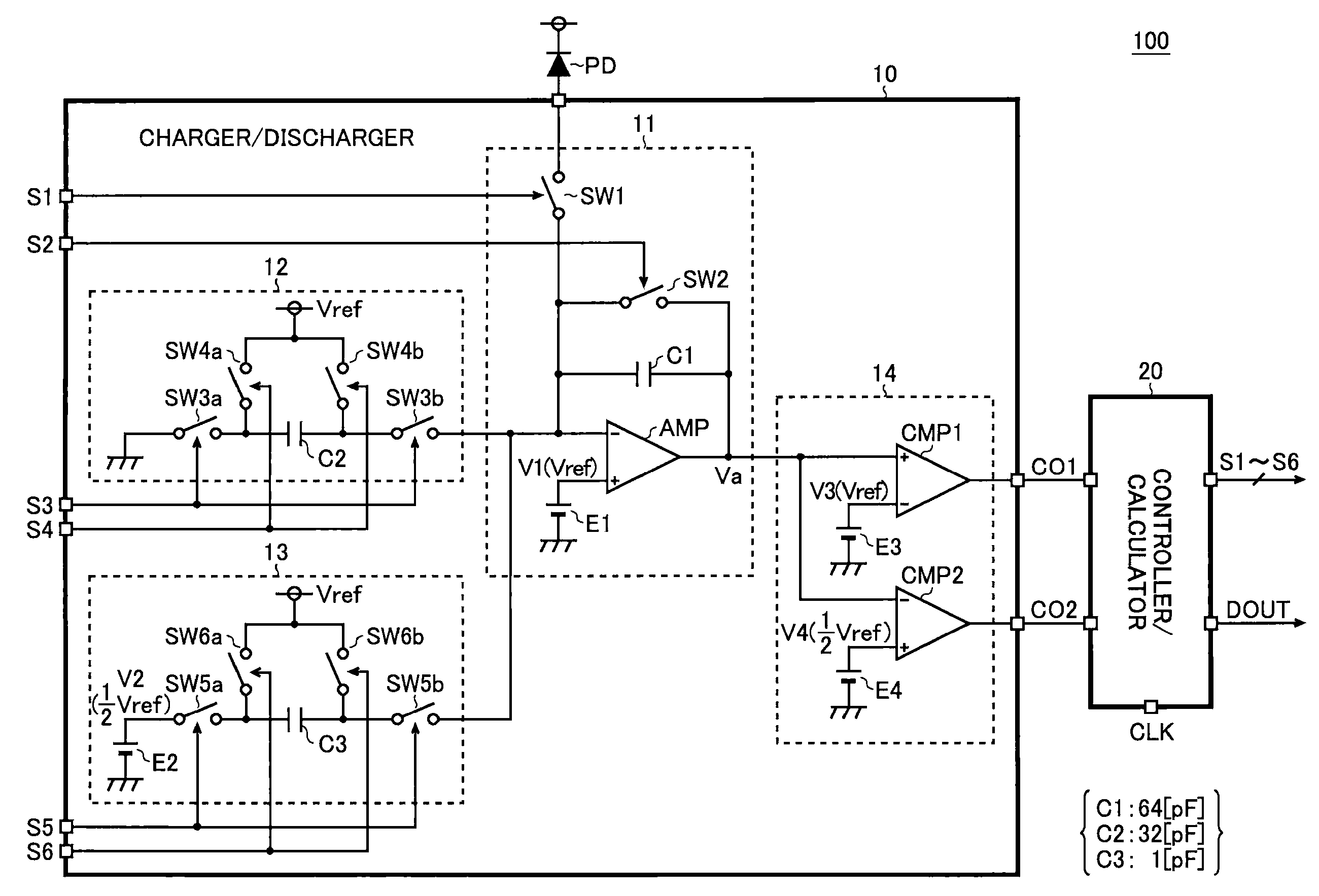
[0029]FIG. 1 is a circuit diagram showing an illuminance sensor according to the invention, as a

[0030]As shown in FIG. 1, the illuminance sensor 100 of this embodiment includes: a photodiode PD that converts measurement-target light into an electric current; and an analog / digital converter (a charger / discharger 10 and a controller / calculator 20) that receives, as an input current to it, the output of the photodiode PD. Thus, the illuminance sensor 100 yields a digital output according to illuminance.

[0031]The charger / discharger 10 includes a charge circuit (integrating operational amplifier) 11, a first discharge circuit 12, a second discharge circuit 13, and a comparison circuit 14.

[0032]The charge circuit 11 stores an electric charge according to an input current (the detection current from the photodiode PD) for a predetermined charge period. The charge circuit 11 includes: an operational amplifier AMP; a charge capacitor C1 (in this embodiment, with a capacitance of 64 pF) of wh...

second embodiment

[0060]FIG. 4 is a circuit diagram showing an illumination sensor according to the invention, as a

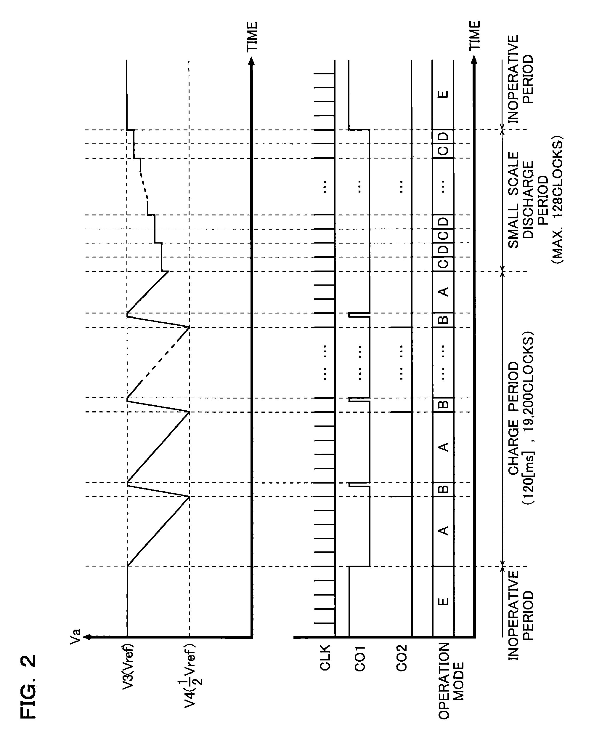
[0061]For example, as shown in FIG. 4, a second discharge circuit 13′ including a constant current circuit I1 and a switch SW5 may be used. In this configuration, after the end of the charge period of the capacitor C1, the switch SW5 is closed so that the electric charge in the capacitor C1 is discharged by the constant current circuit I1 at a predetermined rate; meanwhile, the time that passes until the electric charge in the capacitor C1 decreases to a predetermined level is measured as by counting pulses in the clock signal CLK.

[0062]With this configuration, after coarse measurements are made based on the number of large-scale discharges by the first discharge circuit 12, it is simply necessary to measure, for the small amount of electric charge remaining in the capacitor C1, the discharge duration of the second discharge circuit 13. Thus, even in a case where the input current from t...

third embodiment

[0063]Next, as a third embodiment, another illuminance sensor according to the present invention will be described in detail with reference to FIG. 5.

[0064]FIG. 5 is a circuit diagram showing an illumination sensor according to the invention, as a third embodiment.

[0065]The illuminance sensor 100 of this embodiment has almost the same configuration as those of the first and second embodiments described previously. The unique feature here is that the use of photodiodes PD1 and PD2 having different photodetective characteristics allows measurement of the targeted wavelength alone. In the following description, accordingly, such parts as find their counterparts in the first and second embodiments are identified with reference numerals and symbols common to FIGS. 1 and 4, and no detailed explanation of such parts will be repeated; thus, the following description proceeds with emphasis placed on the features unique to this embodiment.

[0066]As shown in FIG. 5, the illuminance sensor 100 o...


PUM


Abstract

An analog / digital converter has a charge circuit that has a charge capacitor storing an electric charge commensurate with an input current, and first and second discharge circuits that discharge the electric charge stored in the charge capacitor. While the charge capacitor is charged for a predetermined charge period, every time a predetermined amount of electric charge is stored in the charge capacitor, the electric charge stored there is discharged by the first discharge circuit. After the charge period, the electric charge remaining in the charge capacitor is discharged by the second discharge circuit. Based on the number of discharges performed by the first discharge circuit and the discharge duration of the second discharge circuit, a digital value of the voltage commensurate with the amount of electric charge with which the charge capacitor has been charged is outputted. This offers a wider input dynamic range combined with an enhanced minimum resolution without requiring complicated external control, and in addition allows measurement to be performed in less time.

Description

CROSS-REFERENCE TO RELATED APPLICATIONS[0001]This application is based on the following Japanese Patent Applications, the contents of which are hereby incorporated by reference:[0002](1) Japanese Patent Application No. 2006-194422, filed on Jul. 14, 2006; and[0003](2) Japanese Patent Application No. 2007-147648, filed on Jun. 4, 2007.BACKGROUND OF THE INVENTION[0004]1. Field of the Invention[0005]The present invention relates to analog / digital converters, and also relates to illuminance sensors, illumination devices, and electronic devices employing them. More particularly, the present invention concerns with, in such devices, widening the input dynamic range, enhancing the minimum resolution, and shortening the measurement time.[0006]2. Description of Related Art[0007]As a technology related to analog / digital converters, JP-2001-160756 discloses and proposes an analog / digital converter as shown in FIG. 7, comprising a capacitor for storing an electric charge commensurate with a mea...

Claims


Application Information

Patent Timeline
Patent Type & Authority Patents(United States)
IPC IPC(8): H03M1/12
CPCH03M1/14H03M1/54H03M1/60
Inventor NAKATA, YUICHIROFUJINO, JUNJIUEDAIRA, YOSHITSUGU
Owner ROHM CO LTD
Why Eureka
Try Eureka