

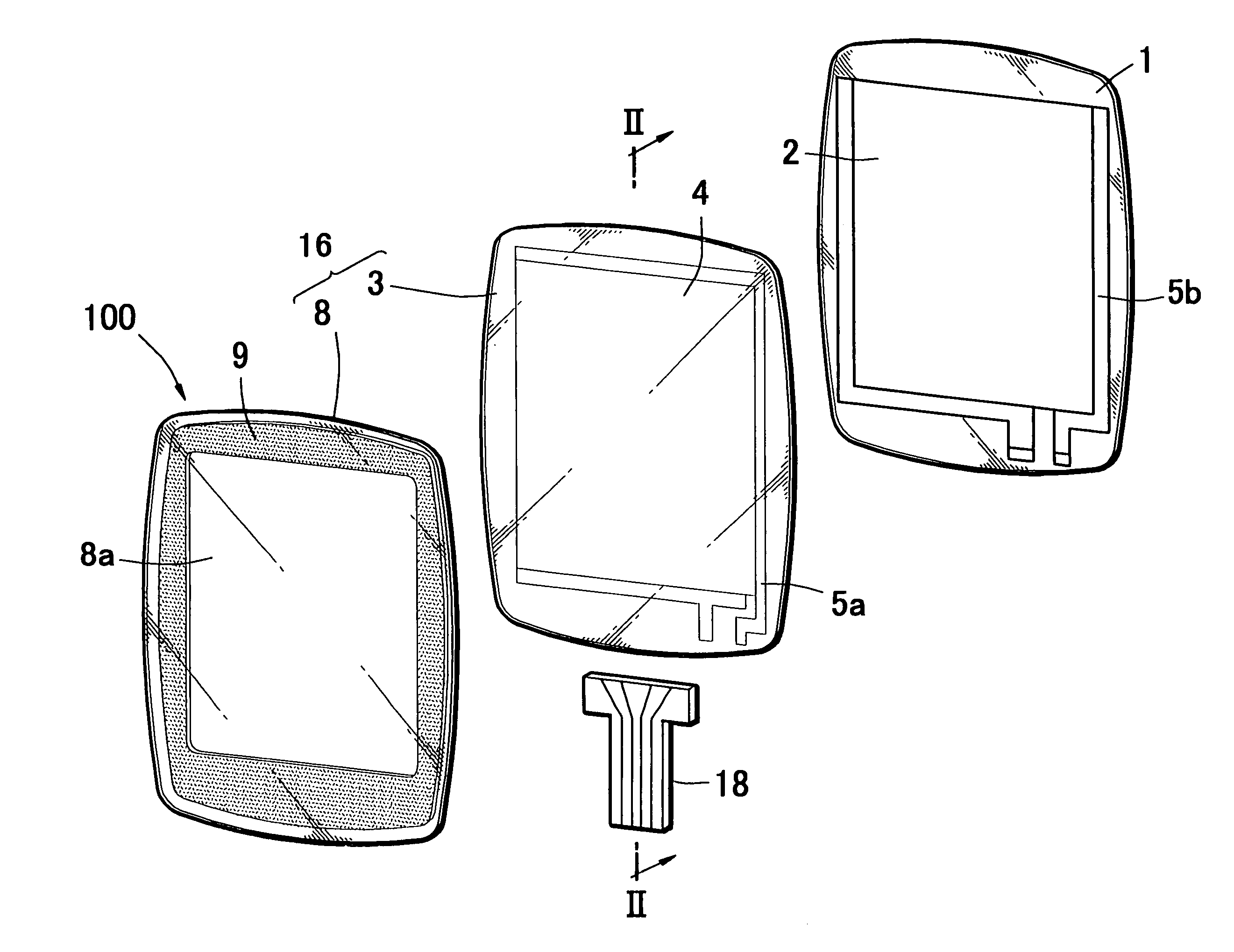
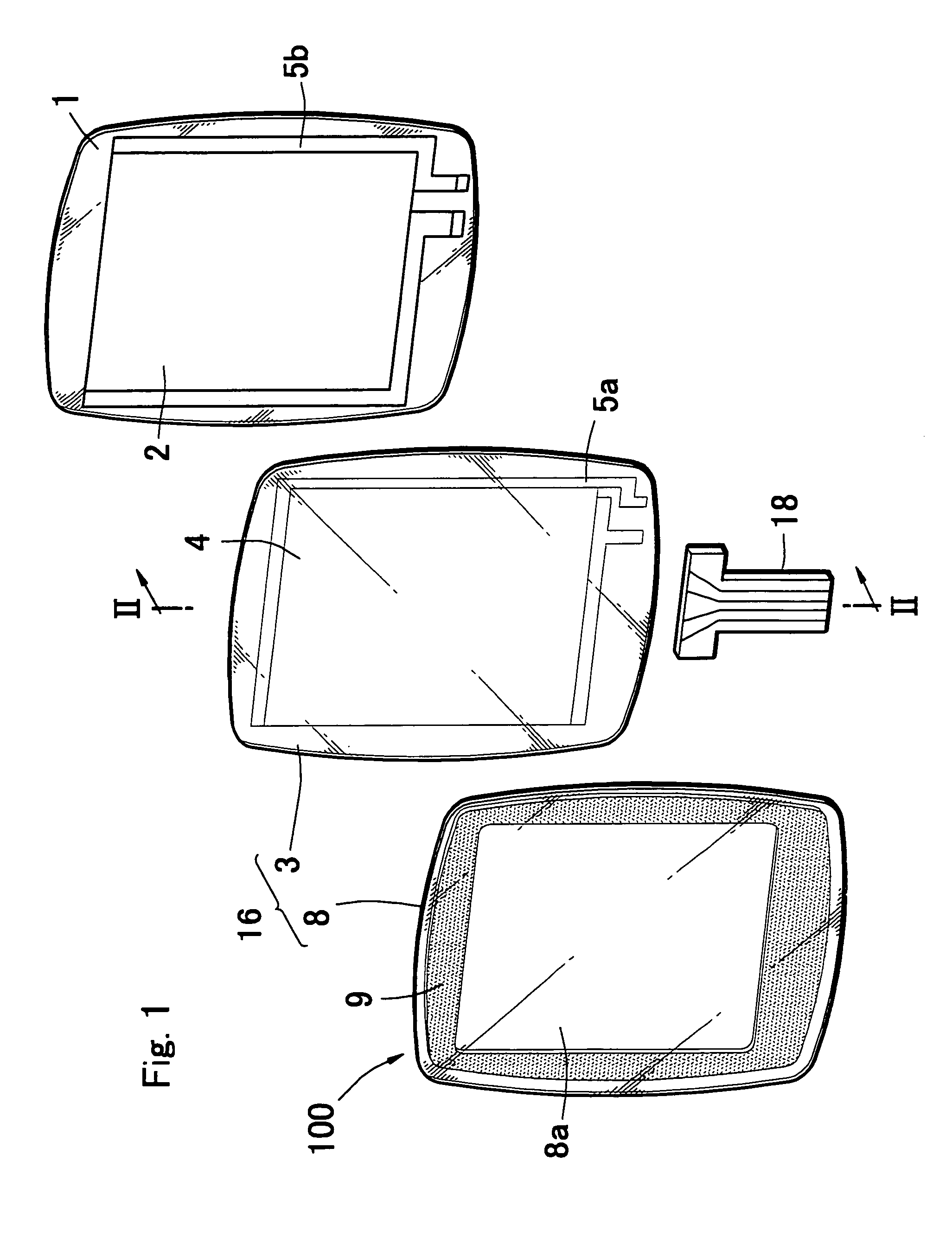
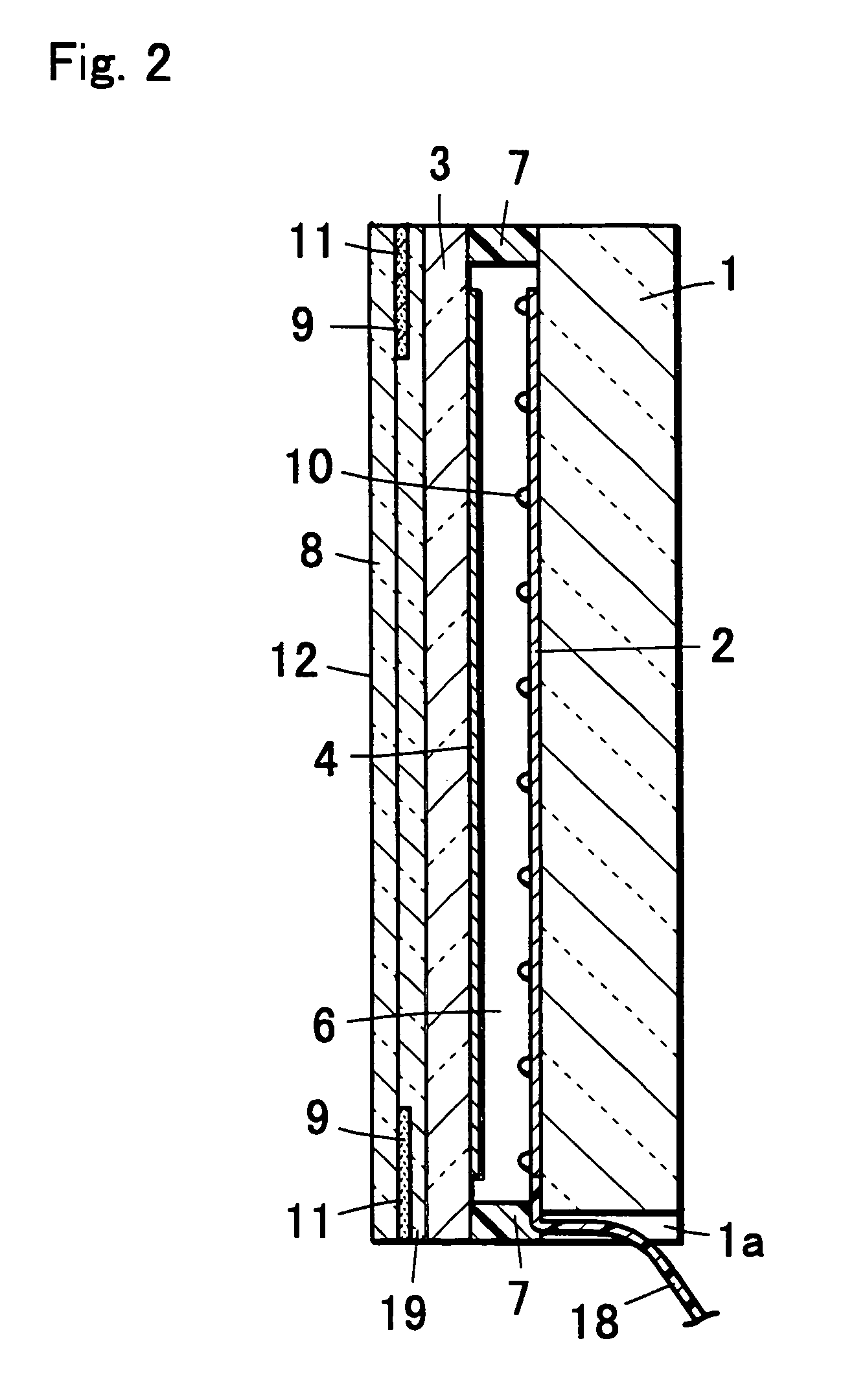
Electronic device with protection panel, protection panel, and method of fabricating protection panels
a technology of electronic devices and protection panels, which is applied in the direction of telephone set constructions, instruments, computing, etc., can solve the problems of difficult to wipe off the edge of the front panel opening b>67/b>, the touch input function is easily degraded, and the touch input function is difficult to be employed. , to achieve the effect of reducing the thickness of the device and avoiding easy degradation of the touch input function
- Summary
- Abstract
- Description
- Claims
- Application Information
AI Technical Summary
Benefits of technology
Problems solved by technology
Method used
Image

Examples
example 1
[0085]An ITO film having a thickness of 20 nm was formed on the entirety of a surface of a PET film having the thickness of 0.1 mm by sputtering. Then, a peripheral portion of the ITO film was removed so that a transparent electrode was obtained in a broad rectangular shape. Bus bars arranged on the two mutually opposing sides in the horizontal direction of the transparent electrode, as well as a circuit for outputting the bus bars to the outside, were formed with silver paste by screen printing. An acrylic plate having the same lateral and vertical dimensions as the above-mentioned PET film and having a thickness of 0.7 mm was bonded to the opposite of the PET film surface on which the transparent electrode was formed, by means of a substrate-less transparent adhesive having a thickness of 0.025 mm. As a result, a fixed electrode board 27 on which a transparent electrode was formed was obtained.
[0086]Further, an ITO film having a thickness of 20 nm was formed by sputtering on the e...
example 2
[0091]The dimensions of the above-mentioned PET based hard coat film were set larger by 5 mm than the circumference of the protection panel main body. Further, before the adhering to the PET film having a thickness of 125 pm, a frame composed of acrylic resin having a thickness of 0.7 mm and a width of 5 mm was integrated into the circumference (of the protection panel main body) by insert molding. Other structures were the same as Example 1.
[0092]In the obtained protection panel, touch input was allowed in the display window of the electronic device such as a portable telephone. The touch input did not slide on the same portion of the operation surface. Further, fouling such as fats and oils was easily wiped off.
[0093]The above-mentioned modes of operation may be combined in an arbitrary manner so that their effects are obtained in combination.
PUM
 Abstract
Description
Claims
Application Information