Supercharge Your Innovation With Domain-Expert AI Agents!

Producing method of wired circuit board

a production method and wired circuit technology, applied in the direction of overvoltage circuit protection, circuit electrostatic discharge protection, non-metallic protective coating application, etc., to achieve the effect of efficiently removing static electricity charged thereon

Inactive Publication Date: 2009-07-07
NITTO DENKO CORP
View PDF9 Cites 0 Cited by
  • Summary
  • Abstract
  • Description
  • Claims
  • Application Information

AI Technical Summary

Benefits of technology

The present invention provides a producing method of a wired circuit board that can prevent discoloration of the terminal portion and efficiently remove static electricity charged on the wired circuit board. The method involves dipping the wired circuit board in a polymeric liquid of a conductive polymer and applying a voltage to form a semiconductive layer on the insulating layer. This semiconductive layer can prevent corrosion in the terminal portion and discoloration while also effectively removing static electricity. The use of a plating layer on the terminal portion is also recommended to further prevent corrosion. The conductive material used in the conductive pattern is copper, which is less likely to dissolve in the polymeric liquid. The voltage applied should be at least 1.0 V to reliably prevent dissolution of the conductive material. The use of polyaniline as the conductive polymer can also improve the efficiency of static electricity removal.

Problems solved by technology

This may corrode the terminal portion, resulting in discoloration therein.

Method used


Image

  • Producing method of wired circuit board
  • Producing method of wired circuit board
  • Producing method of wired circuit board

Examples


example 1

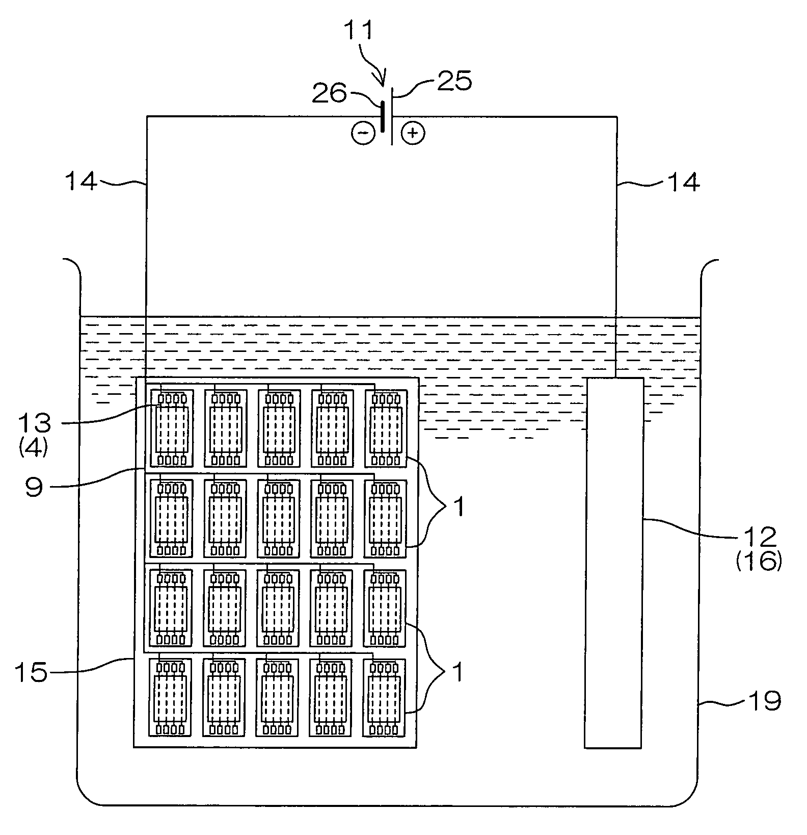
[0126]A metal supporting board made of a 20 μm thick stainless steel was prepared (cf. FIG. 4(a)).

[0127]Subsequently, a varnish of photosensitive polyamic acid resin was uniformly coated over an upper surface of the metal supporting board using a spin coater. The coated varnish was then heated at 90° C. for 15 minutes to form a base coating. Thereafter, the base coating was exposed to light at 700 mJ / cm2 via a photomask, and then heated at 190° C. for 10 minutes. The base coating thus heated was then developed using an alkaline developer. Subsequently, the coating was cured at 385° C. under the pressure reduced to 1.33 Pa, thereby forming an insulating base layer of polyimide on the metal supporting board in a pattern corresponding to each suspension board with circuit (cf. FIG. 4(b)). The insulating base layer thus formed had a thickness of 10 μm.

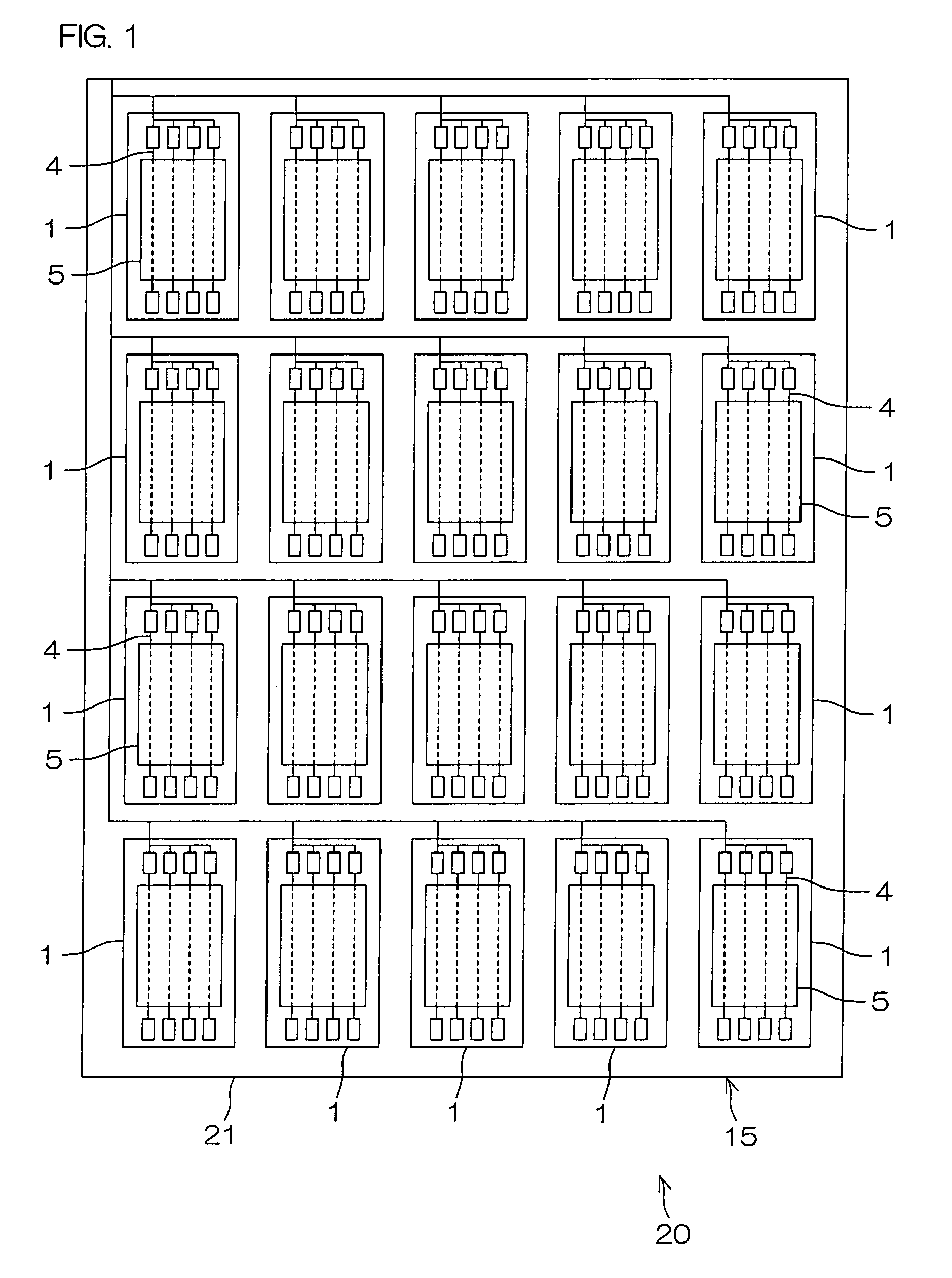
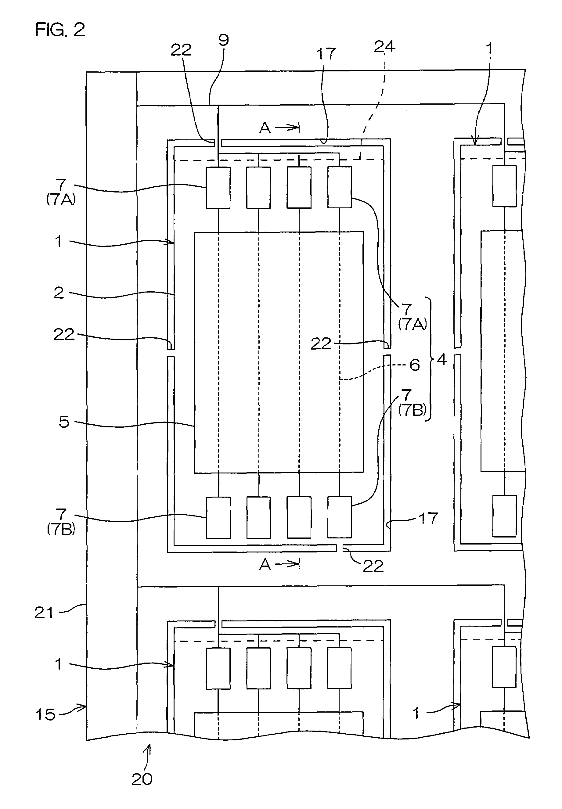
[0128]Next, by an additive method, a conductive pattern made of a 15 μm thick copper was formed in the pattern corresponding to each of t...

example 2

[0138]The plurality of suspension boards with circuit were obtained in the same method as in Example 1 except that the voltage applied was changed from 1.0 V to 1.5 V in Example 1.

example 3

[0139]The plurality of suspension boards with circuit were obtained in the same method as in Example 1 except that the voltage applied was changed from 1.0 V to 2.0 V in Example 1.


PUM


Abstract

A producing method of a wired circuit board includes the step of preparing a wired circuit board including an insulating layer and a conductive pattern having a wire covered with the insulating layer and a terminal portion exposed from the insulating layer; and the step of forming a semiconductive layer on a surface of the insulating layer by dipping the wired circuit board in a polymeric liquid of a conductive polymer in which an electrode is provided, and applying a voltage so that the electrode becomes an anode and the conductive pattern becomes a cathode.

Description

CROSS-REFERENCE TO RELATED APPLICATION[0001]This patent application claims the benefit of U.S. Provisional Application No. 60 / 907,024, filed on Mar. 16, 2007, and claims priority from Japanese Patent Application No. 2006-294620, filed on Oct. 30, 2006, the contents of which are herein incorporated by reference in their entirety.BACKGROUND OF THE INVENTION[0002]1. Field of the Invention[0003]The present invention relates to a producing method of a wired circuit board. More particularly, the present invention relates to a producing method of a wired circuit board such as a suspension board with circuit.[0004]2. Description of the Related Art[0005]There has been conventionally known a wired circuit board on which an insulating base layer, a conductive pattern having a wire and a terminal portion, and an insulating cover layer are sequentially laminated. The wired circuit boards of this type are widely used in a variety of fields of electric and electronic equipment.[0006]As a producing...

Claims


Application Information

Patent Timeline
Patent Type & Authority Patents(United States)
IPC IPC(8): H01L21/31
CPCH05K1/0259H05K2203/135H05K2201/0329H05K3/28
Inventor ISHII, JUNOOYABU, YASUNARIKURAI, HIROYUKI
Owner NITTO DENKO CORP
Features
  • R&D
  • Intellectual Property
  • Life Sciences
  • Materials
  • Tech Scout
  • Unparalleled Data Quality
  • Higher Quality Content
  • 60% Fewer Hallucinations
Learn More