
Display and method for manufacturing the same

a technology of display and manufacturing method, applied in the field of display, can solve the problems of low performance, achieve the effects of enhancing the resolution of the conductor, preventing separation or damage of the conductor, and high bonding strength

Active Publication Date: 2009-07-07
SAMSUNG DISPLAY CO LTD
View PDF13 Cites 16 Cited by
  • Summary
  • Abstract
  • Description
  • Claims
  • Application Information

AI Technical Summary

Benefits of technology

The present invention provides a display with a substrate and electrode layer that have a plurality of conductors, with a silane derivative layer interposed between the substrate and electrode layer. This results in a high bond strength between the conductors and the substrate, enhancing the resolution of the conductors and preventing separation or damage. The method of manufacturing the display involves preparing a substrate, forming a silane derivative layer on the substrate, and forming an electrode layer comprising a plurality of conductors on the silane derivative layer. This results in a display with improved performance and resolution.

Problems solved by technology

This configuration enhances the resolution of the conductors inkjet-printed on the glass or the ITO substrate and prevents the separation or damage to the conductors which causes product defects and results in low performance.

Method used


Image

  • Display and method for manufacturing the same
  • Display and method for manufacturing the same
  • Display and method for manufacturing the same

Examples


example

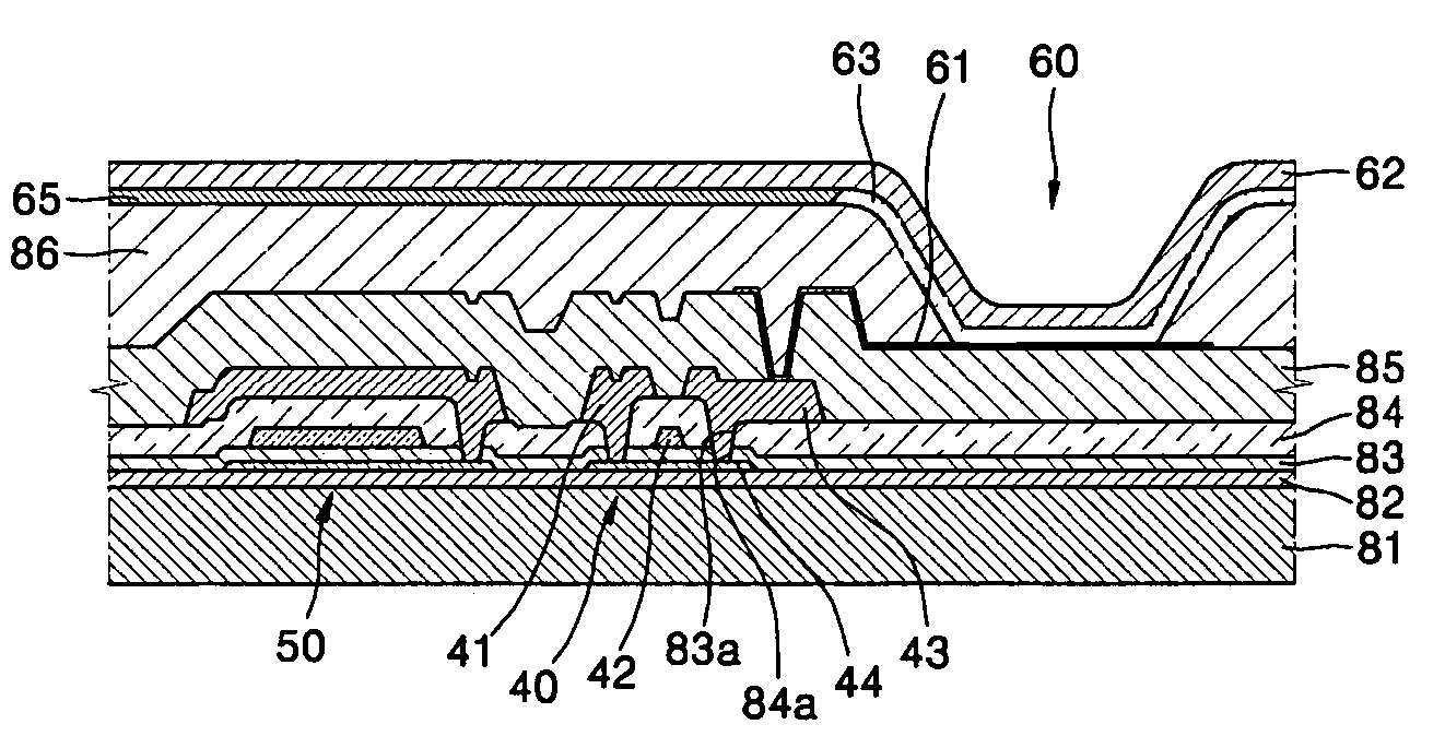
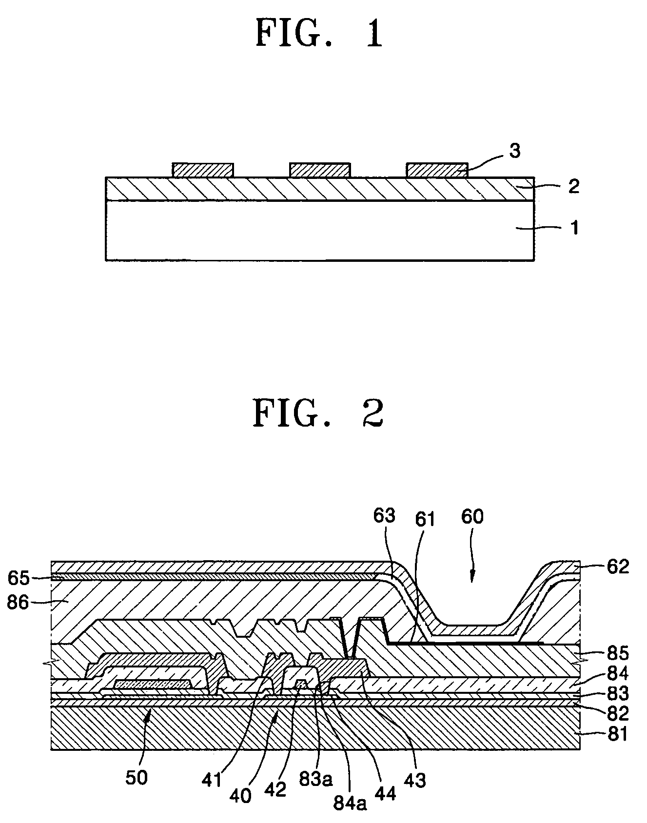
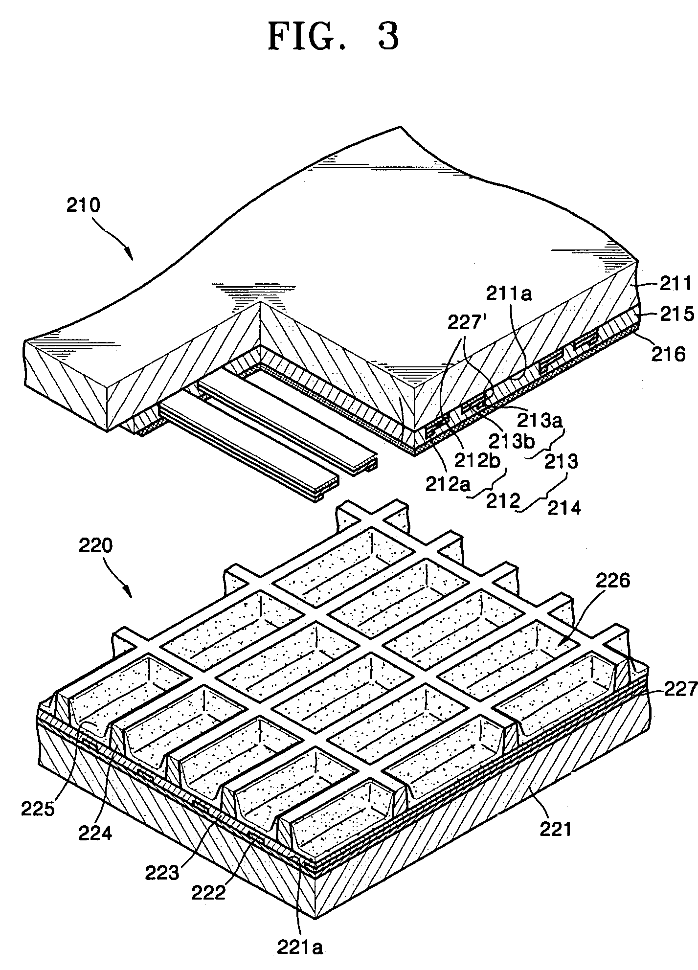
[0074]In this example, a PDP including a substrate, an electrode layer including a plurality of conductors, and a silane derivative layer interposed between the substrate and the electrode layer is fabricated. Bus and address electrodes of the PDP are formed on two different substrates, which may be a glass substrate (for address electrodes) and an ITO-coated glass substrate (for bus electrodes).

[0075]First, a washed glass substrate was prepared.

[0076]The washed glass substrate was subjected to plasma polymerization method such as PECVD using HMDSO (hexamethyldisiloxane) to form a silane derivative layer with a thickness of 5 nm. The contact angle of silver ink droplets on the silane derivative layer was about 30 degrees. At this time, parameters for the plasma polymerization are listed in Table 1 below:

[0077]

TABLE 1Pressure5 × 10−2mbarPower200WRF-frequency13.56MHzFlow rate of HMDSO (monomer)5.5sccmTime10seconds

[0078]A dispersion of silver nanoparticles with a particle size of about...


PUM

PropertyMeasurementUnit
thicknessaaaaaaaaaa
thicknessaaaaaaaaaa
contact angleaaaaaaaaaa

Abstract

The present invention provides a display including a substrate and an electrode layer including a plurality of conductors, wherein a silane derivative layer is interposed between the substrate and the electrode layer to increase the bond strength between the substrate and the electrode layer. The invention also provides a method of manufacturing the device.

Description

CROSS REFERENCE TO RELATED APPLICATION[0001]This application claims priority to and benefit of German Patent Application No. DE 10 2004 037 524.0, filed on Jul. 29, 2004, in the German Patent Office and Korean Patent Application No. 10-2004-0098823, filed on Nov. 29, 2004, in the Korean Patent Office, the disclosures of which are incorporated herein in their entireties by reference.BACKGROUND OF THE INVENTION[0002]1. Field of the Invention[0003]The present invention relates to a display, and more particularly, to a display that includes a substrate, an electrode layer that has a plurality of conductors, and a silane derivative layer that is interposed between the substrate and the electrode layer. The silane derivative layers enhance the bond strength between the substrate and the electrode layer. The present invention also relates to a method for manufacturing the display.[0004]2. Description of the Background[0005]Inkjet-printed bus electrodes and address electrodes are printed us...

Claims


Application Information

Patent Timeline
Patent Type & Authority Patents(United States)
IPC IPC(8): H01L35/24H01L51/00H10N10/856
CPCH01J9/02H01J11/12H01J11/22H01L27/3244H01L51/0005H01J2211/225H01L51/5221H01L27/3246H01L51/5206H01L27/1214H05K1/0306H05K3/389H10K59/122H10K71/135H10K59/8051H10K59/8052H10K59/12H10K50/81H10K50/82
Inventor HUMBS, WERNERREDECKER, MICHAELSCHAEDIG, MARKUS
Owner SAMSUNG DISPLAY CO LTD
Learn More