Method of designing a synchronous circuit of VLSI for clock skew scheduling and optimization

a technology of synchronous circuit and clock skew, applied in multi-objective optimization, instruments, cad techniques, etc., can solve the problems of increasing the difficulty of high-performance integrated circuit design and raising the so as to improve the reliability and performance of the circuit, speed up the operation, and reduce the complexity

a technology of synchronous circuit and clock skew, applied in multi-objective optimization, instruments, cad techniques, etc., can solve the problems of increasing the difficulty of high-performance integrated circuit design and raising the so as to improve the reliability and performance of the circuit, speed up the operation, and reduce the complexity

US7562324B2Inactive Publication Date: 2009-07-14CHANG GUNG UNIVERSITY

Image

  • Method of designing a synchronous circuit of VLSI for clock skew scheduling and optimization
  • Method of designing a synchronous circuit of VLSI for clock skew scheduling and optimization
  • Method of designing a synchronous circuit of VLSI for clock skew scheduling and optimization

Examples


Embodiment Construction

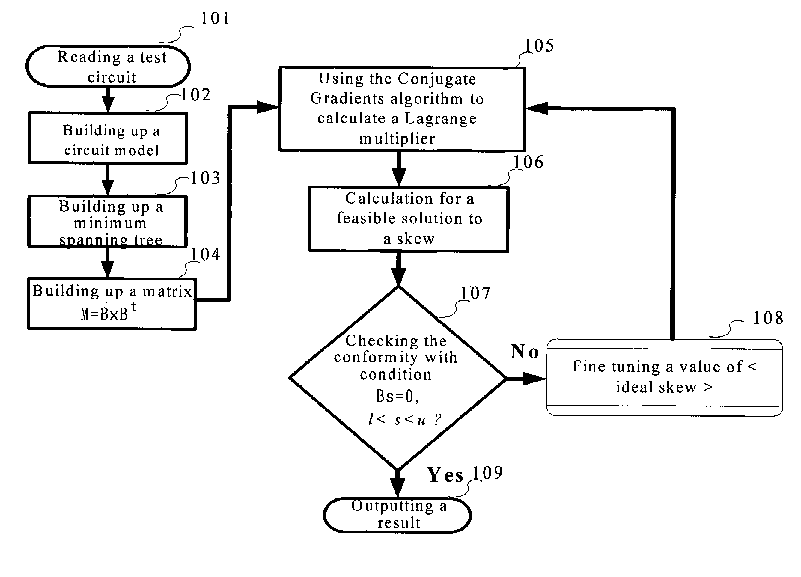
[0028]Now, the present invention will be described more specifically with reference to the following embodiments. It is to be noted that the following descriptions of preferred embodiments of this invention are presented herein for purpose of illustration and description only; it is not intended to be exhaustive or to be limited to the precise form disclosed.

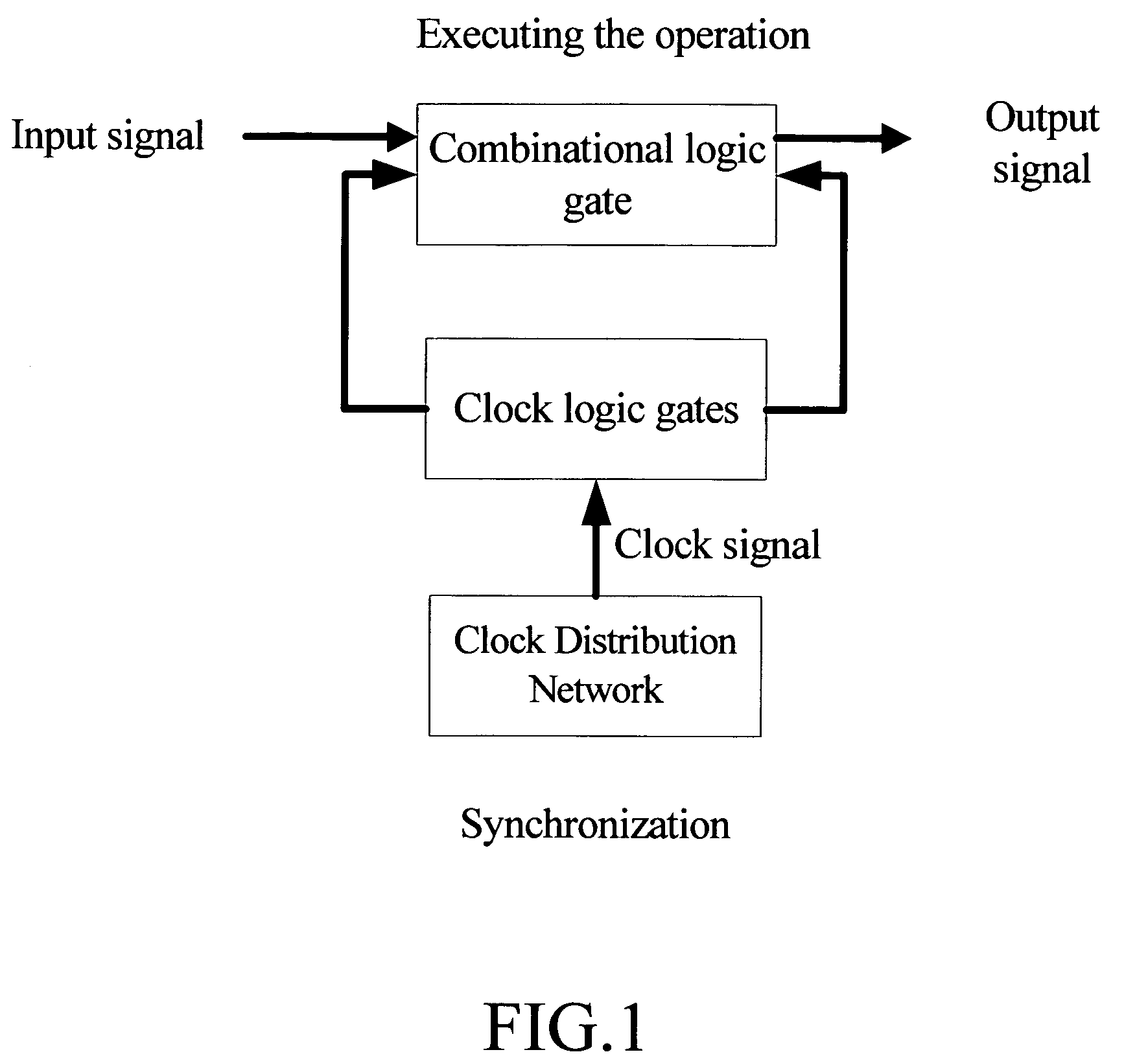
[0029]Generally speaking, a digital synchronous VLSI system proposed in a conventional technology comprises three elements:[0030]1. combinational logic circuit, a primary circuit for a system to execute the operation, comprising several logic gates;[0031]2. clock-based storage element that is made up with registers to store results given from the operation by the logic circuit;[0032]3. Clock Distribution Network providing the input of clock-based storage element, which coordinates the synchronization of system by means of the control of time difference, the synchronous system being shown in FIG. 1.

Clock Skew and Security Range

[0...


PUM


Abstract

A method of designing a synchronous circuit of VLSI for Clock Skew scheduling and optimization is used to optimize the skew of a digital synchronous VLSI system and formulize the issue of skew optimization into the issue of quadratic equation programming. For estimation of reliability, a quadratic equation cost function is used to analyze an ideal value of skew and an error between feasible solutions. During operation, several algorithms are used to speed up the operation and lower the complexity, and ISCAS'89 is used as a testing circuit.

Description

BACKGROUND OF THE INVENTION[0001]1. Field of the Invention[0002]This invention relates to optimization of the skew of a digital synchronous VLSI system and particularly to the acceleration of operation speed and the reduction of complexity.[0003]2. Description of Related Art[0004]Along with nano-technology that prevails, what is concerned in a high-performance integrated circuit design includes higher design complexity, high-speed clock frequency, lower interconnect width, and lower Supply Voltage, which increases the difficulty of high-performance integrated circuit design. Besides speed and surface area, reliability must be considered for the critical target of optimization.[0005]A high-frequency digital synchronous VLSI circuit operates with a region assembly logic circuit, in this way, registers must be arranged in a specified region of the circuit and are controlled by clock signals; if the digital synchronous circuit is made to operate normally, the clock signals must be trans...

Claims


Application Information

Patent Timeline
14 Jul 2009
Publication
US7562324B2
IPC
G06F17/50
CPC
G06F17/5031; G06F17/505; G06F2217/62; G06F2217/08; G06F2111/06; G06F30/3312; G06F30/396; G06F30/327
Inventors
CHANG, CHAO-KAI; CHU, CHIA-CHI