Controllable delay line and regulation compensation circuit thereof

a delay line and control circuit technology, applied in the direction of multiple-port active networks, active elements, electrical devices, etc., can solve the problems of limited operation speed and maximum delay, high design cost, limited operation speed, etc., to reduce the jitter amount of output signal, reduce the influence of transition, and reduce the variation of voltage

Inactive Publication Date: 2009-07-21
FARADAY TECH CORP
View PDF3 Cites 5 Cited by
  • Summary
  • Abstract
  • Description
  • Claims
  • Application Information

AI Technical Summary

Benefits of technology

[0008]Accordingly, the present invention is directed to provide a controllable delay line able to reduce the influence of a power voltage variation on the bias voltage source thereof.
[0009]The present invention is further directed to provide a controllable delay line able to reduce the influence of a power voltage variation on the jitter of an output signal.
[0010]The present invention is further yet directed to provide a controllable delay line able to increase the operation speed and the maximum delay thereof.
[0012]The present invention further provides a regulation compensation circuit suitable for a controllable delay line, wherein the controllable delay line includes a first current source and an output buffer unit, while the regulation compensation circuit includes a regulation capacitor and a compensation capacitor. The regulation capacitor is for reducing a variation of the voltage between a voltage source and a node of the first current source. The compensation capacitor is coupled between the node of the first current source and the output buffer unit. When an input signal of the output buffer unit gets a transition, the compensation capacitor can reduce the influence of the transition on the voltage of the node so as to reduce the jitter amount of the output signal of the output buffer unit.

Problems solved by technology

Controllable delay lines in the conventional design, however, are vulnerable by power voltage variation and have higher design cost, limited operation speed and limited maximum delay.

Method used


Image

  • Controllable delay line and regulation compensation circuit thereof
  • Controllable delay line and regulation compensation circuit thereof
  • Controllable delay line and regulation compensation circuit thereof

Examples


Embodiment Construction

[0019]In order to better understand the present invention, an embodiment thereof is exemplarily described in detail as the following.

[0020]In the present invention, an anti-jitter unit is employed to increase the circuit reliability and reduce the jitter amount. In addition, a compensation capacitor is employed to reduce the jitter amount of the output signal and a regulation capacitor is employed to reduce the voltage variation inside the circuit.

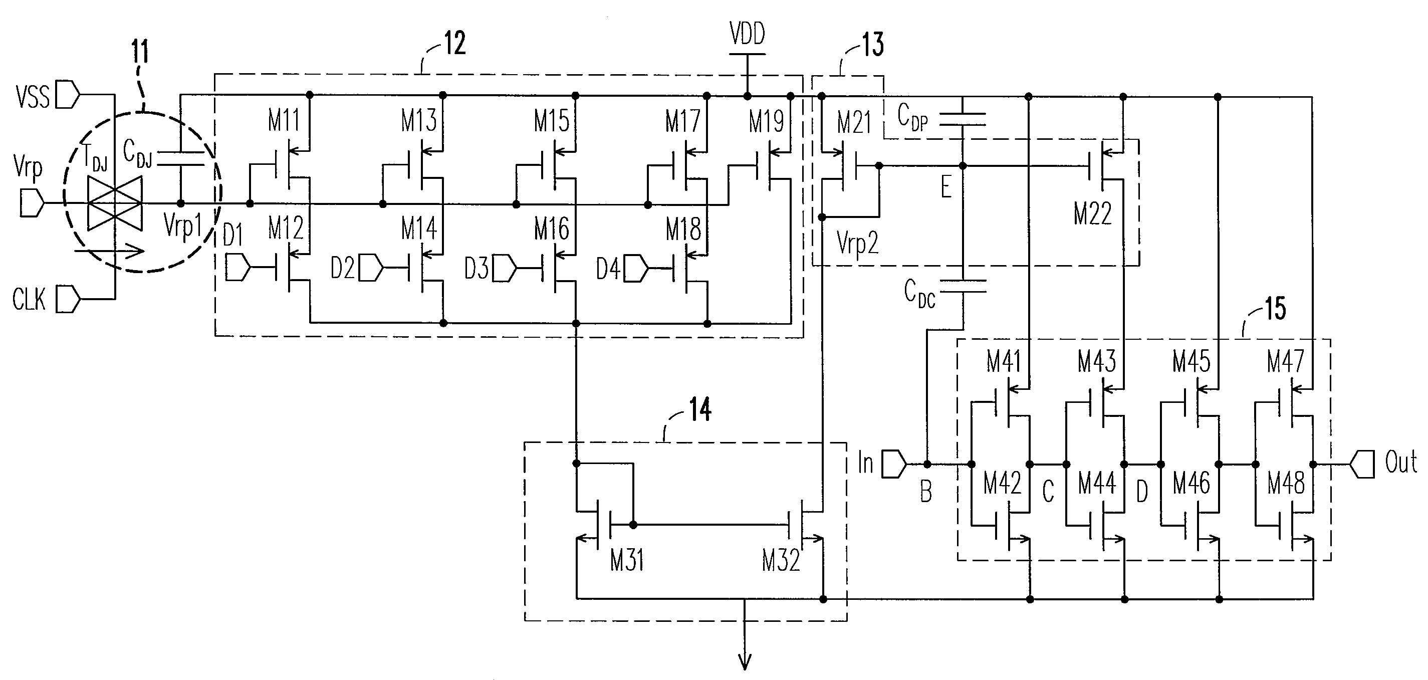
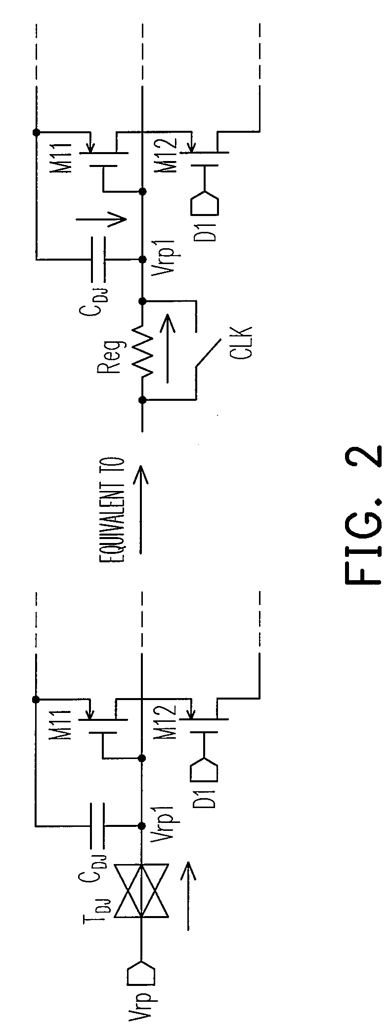
[0021]FIG. 1 is a circuit diagram of a controllable delay line according to an embodiment of the present invention. As shown by FIG. 1, the controllable delay line of the present embodiment includes an anti-jitter unit 11, a dependent current source 12, current mirrors 13 and 14, a regulation capacitor CDP, a compensation capacitor CDC and an output buffer unit 15.

[0022]The anti-jitter unit 11 includes a transmission gate TDJ and a capacitor CDJ. When a voltage source VDD has a variation (for example, ±10% variation), the anti-jitter unit ...


PUM


Abstract

A controllable delay line includes an anti-jitter unit, a dependent current source, a first current mirror, a second current mirror, a regulation capacitor, a compensation capacitor and an output buffer unit. The anti-jitter unit receives a first bias voltage and produces a second bias voltage based on the first bias voltage. When the voltage source used in the controllable delay line has a variation, the second bias voltage varies therewith. The regulation capacitor is used for reducing the variation of the voltage difference between the voltage source and a node voltage of the first current source. The compensation capacitor is used for reducing the influence of a transition of the input signal of the output buffer unit on the node voltage, so as to lower the jitter amount of the output signal of the output buffer unit.

Description

CROSS-REFERENCE TO RELATED APPLICATION[0001]This application claims the priority benefit of Taiwan application serial no. 96104474, filed Feb. 7, 2007. All disclosure of the Taiwan application is incorporated herein by reference.BACKGROUND OF THE INVENTION[0002]1. Field of the Invention[0003]The present invention relates to a controllable delay line.[0004]2. Description of Related Art[0005]Delay lines can be used in many applications, such as in phase-locked loops, delay-locked loops or time interval measuring. In addition, delay lines can be used in jitter measuring of PLL or DLL as well.[0006]Controllable delay lines in the conventional design, however, are vulnerable by power voltage variation and have higher design cost, limited operation speed and limited maximum delay.[0007]Based on the above-mentioned situation, such a controllable delay line is preferred that any influence caused by power voltage variation would be reduced and the operation speed and the maximum delay thereo...

Claims


Application Information

Patent Timeline
Patent Type & Authority Patents(United States)
IPC IPC(8): H03H11/26
CPCH03H11/265
Inventor CHANG, CHIA-WEICHANG, YEONG-JAR
Owner FARADAY TECH CORP
Why Eureka
Try Eureka