Liquid phase deposition of contacts in programmable resistance and switching devices

a technology of programmable resistance and switching device, applied in the direction of semiconductor/solid-state device manufacturing, basic electric elements, electric apparatus, etc., can solve the problems of increasing the difficulty of processing devices, limiting the goal of device miniaturization, and difficult to define small-scale features, etc., to reduce programming current, reduce structural irregularities, and increase the density and resistivity of devices

Active Publication Date: 2009-07-28
OVONYX MEMORY TECH LLC
View PDF2 Cites 62 Cited by
  • Summary
  • Abstract
  • Description
  • Claims
  • Application Information

AI Technical Summary

Benefits of technology

[0023]In accordance with one embodiment of the instant invention, a programmable resistance material or switching material deposition is performed utilizing a chemical solution-based deposition process to selectively and conformally fill the insulative layer opening to the conductive bottom composite electrode layer. Conformally filling the conductive material within the opening reduces structural irregularities within the opening thereby increasing material density and resistivity within the device and thereby reducing programming current.

Problems solved by technology

One of the significant practical challenges that the programmable resistance memory and switching devices face is to reduce the contact area of one or more electrodes contacting the chalcogenide material.
Lithography is commonly used to define small-scale features of semiconductor devices and often sets a limit on the goal of device miniaturization.
As the feature size of devices is minimized, however, processing of the devices becomes more difficult.
Small scale features become more difficult to define as the lithographic limit of resolution is reached and features that are defined become more difficult to process.
As the dimension or length scale of an opening decreases upon miniaturization, it becomes increasingly difficult to satisfactorily fill the opening with another material.
Techniques such as physical vapor deposition (PVD) or sputtering fail to provide dense or complete filling of openings when the dimensions of the opening are reduced below a critical size.
Instead of providing a dense, uniform filling, these techniques increasingly incompletely fill openings as the dimension of the opening decreases while the depth stays the same, thus increasing the aspect ratio.
Lack of structural uniformity in the filling of openings compromises device functionality as variations occur from device-to-device across an array of devices on a substrate.
In addition, less than optimal performance is achieved for each device due to the defective nature of the deposited material.
Deep, narrow channels, for example, are more difficult to uniformly fill than channels that are shallow and wide.
With deep, narrow features, sputtering and other physical deposition techniques are oftentimes unable to deliver sufficient material to the bottom of the feature.
Conformality of deposition is another processing difficulty that becomes exacerbated as feature size decreases.
In addition to difficulties with achieving uniform filling, openings also present complications for achieving conformal deposition that become more pronounced as size of the opening decreases.
Achieving conformality over discontinuous features becomes increasingly difficult as the feature size of the opening decreases or the aspect ratio of the opening increases.
The imperfections detract from device performance.
Although CVD in principle is a viable strategy for forming lithographic or sublithographic contacts in programmable resistance and switching devices, the technique is limited in practice because of the unavailability of gas phase precursors for a variety of desirable contact materials.
In addition, the reaction conditions (e.g. high temperatures or plasma conditions) needed to react the precursors may damage other layers in the device structure.

Method used


Image

  • Liquid phase deposition of contacts in programmable resistance and switching devices
  • Liquid phase deposition of contacts in programmable resistance and switching devices
  • Liquid phase deposition of contacts in programmable resistance and switching devices

Examples


Embodiment Construction

[0035]The making and using of the presently preferred embodiments are discussed in detail below. It should be appreciated, however, that the present invention provides many applicable inventive concepts that can be embodied in a wide variety of specific contexts. The specific embodiments discussed are merely illustrative of specific ways to make and use the invention, and do not limit the scope of the invention.

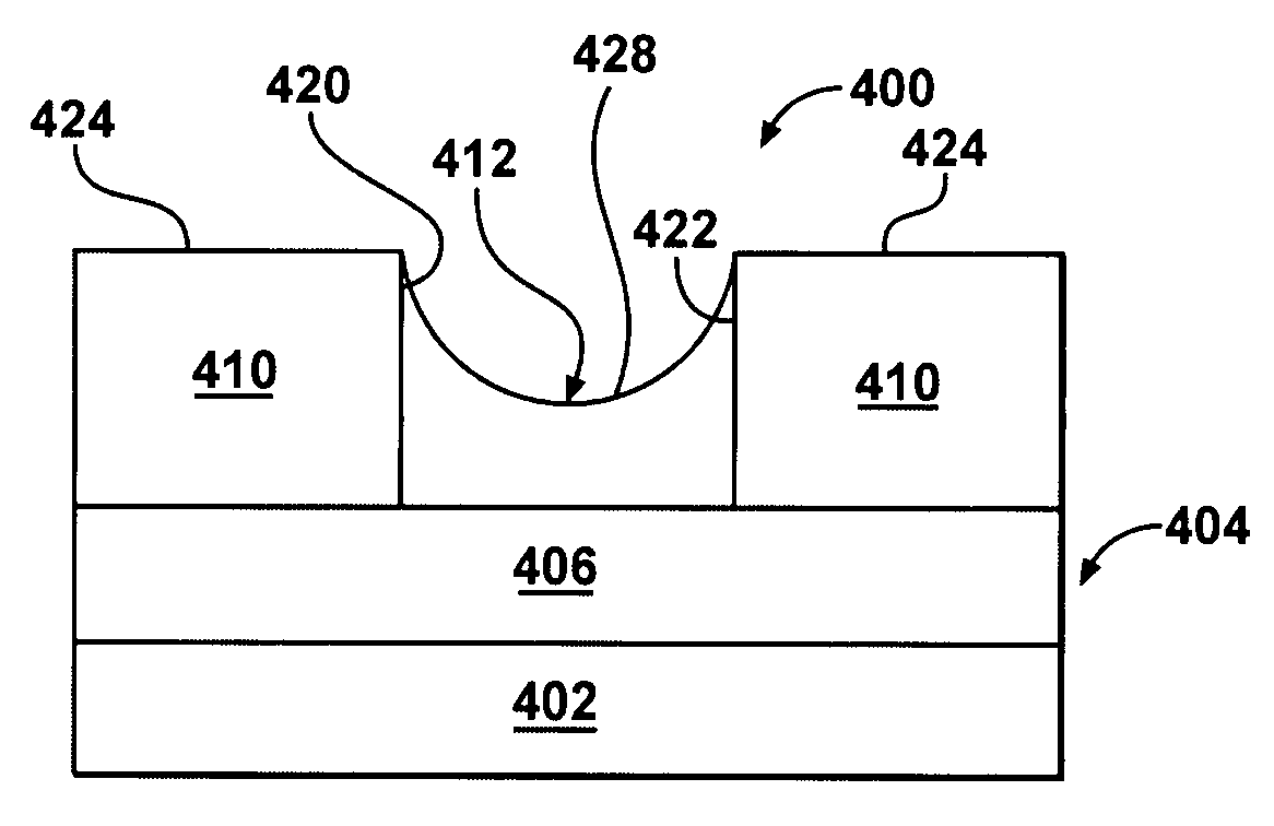
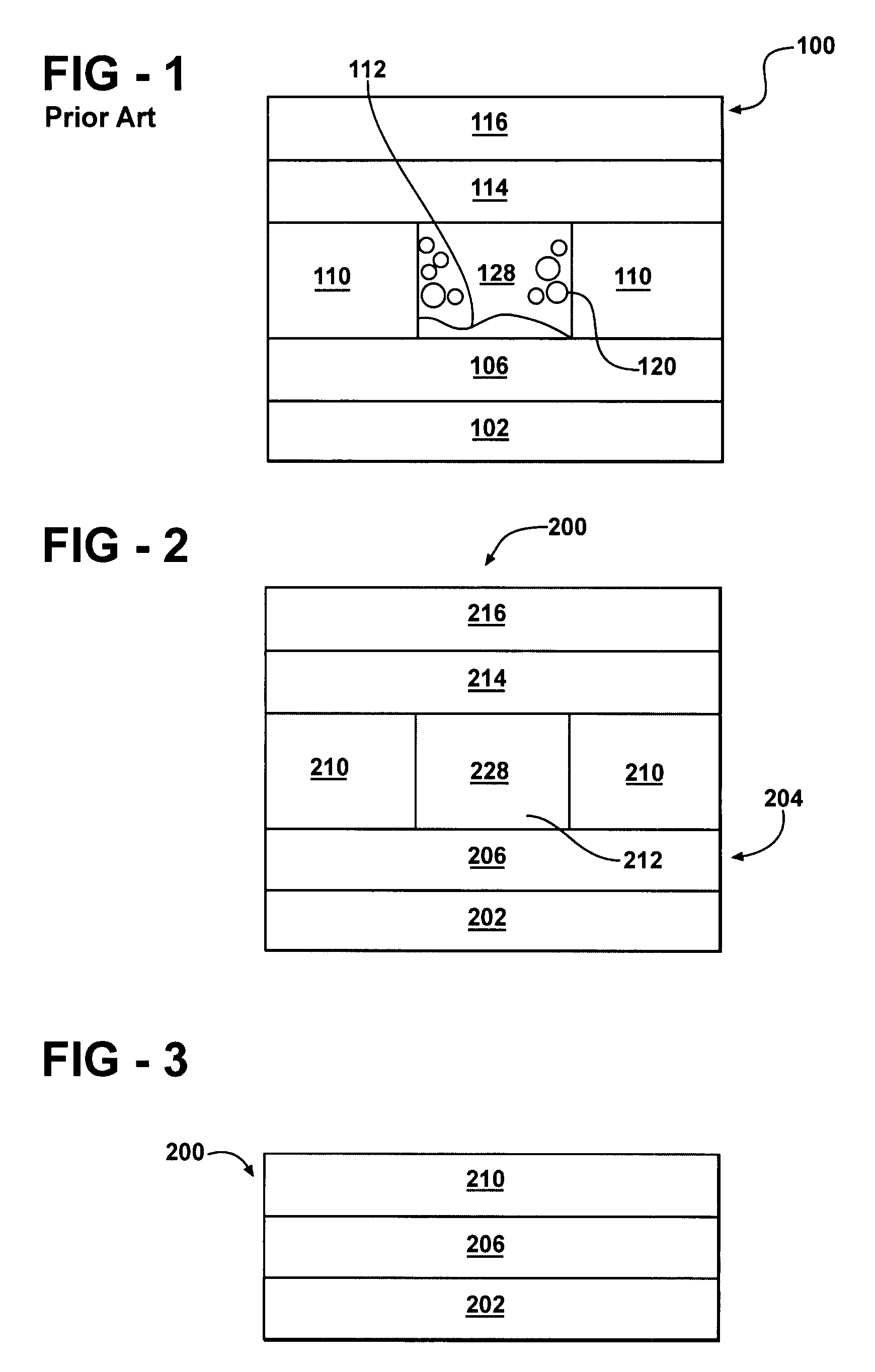
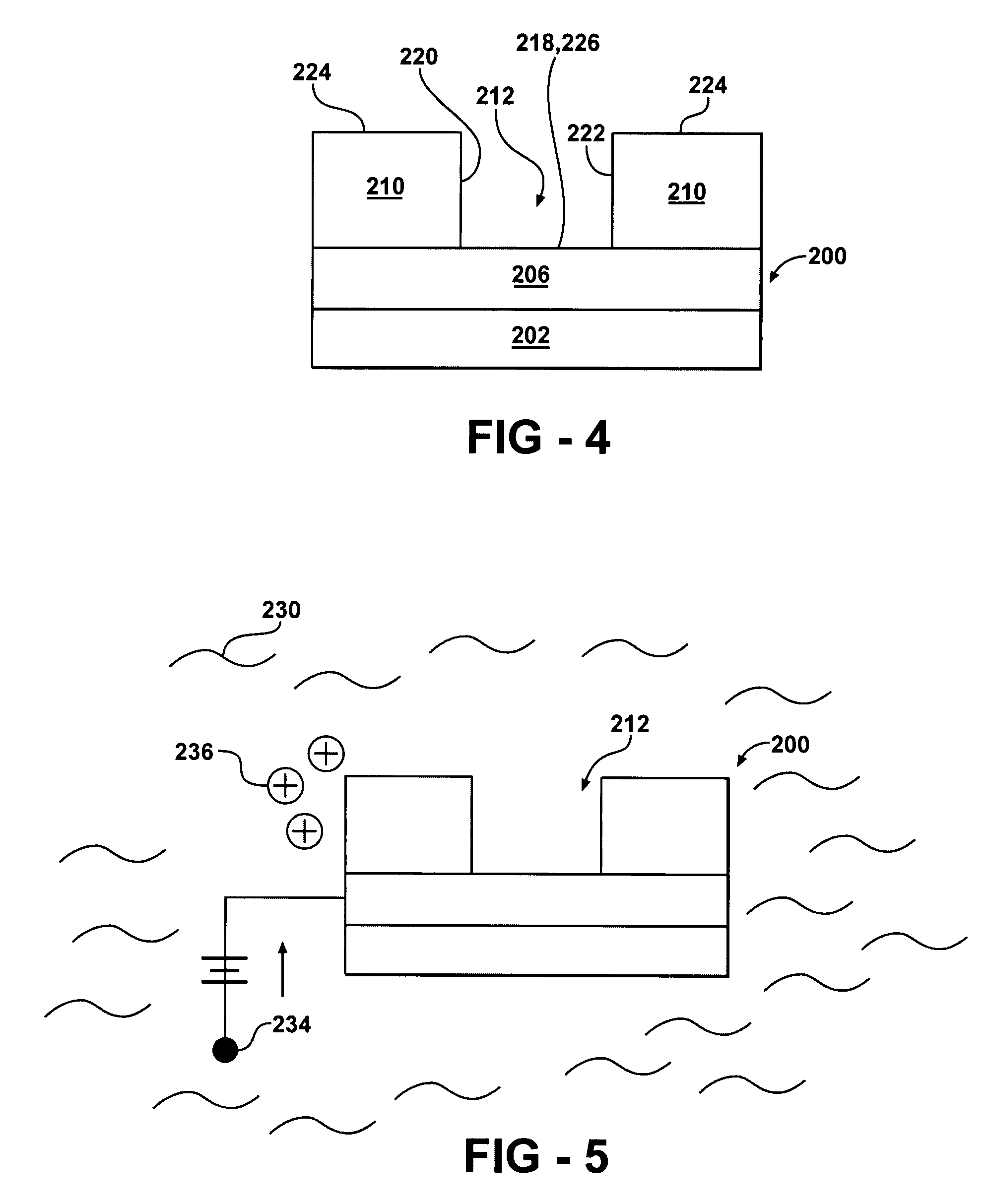
[0036]The intermediate stages of manufacturing a novel electronic device including an active material in accordance with the instant invention are illustrated in FIGS. 2 through 9. Throughout the various views and illustrative embodiments of the instant invention, like reference numbers are used to designate like elements.

[0037]As used herein, active material refers generally to an electrically stimulable material such as a programmable resistance material or an electrical switching material. A programmable resistance material is a material having two or more states that are ...


PUM


Abstract

A programmable resistance, chalcogenide, switching or phase-change material device includes a substrate with a plurality of stacked layers including a conducting bottom composite electrode layer, an insulative layer having an opening formed therein, an active material layer deposited over both the insulative layer and the bottom composite electrode, and a top electrode layer deposited over the active material layer. The device uses a chemical or electrochemical liquid phase deposition process to selectively and conformally fill the insulative layer opening with the conductive bottom composite electrode layer. Conformally filling the conductive material within the opening reduces structural irregularities within the opening thereby increasing material density and resistivity within the device and thereby improving device performance and reducing programming current.

Description

FIELD OF INVENTION[0001]This invention relates generally to programmable resistance and switching devices having one or more electrical contacts with a lithographic or sublithographic dimension. More particularly, this invention relates to programmable resistance and switching device structures with contacts formed from solution-based deposition methods. Most particularly, this invention relates to programmable resistance and switching devices with sublithographic contacts having reduced structural irregularities, improved conformality, and reduced programming currents.BACKGROUND OF THE INVENTION[0002]Programmable resistance materials and fast switching materials are promising active materials for next-generation electronic storage, computing and signal transfer devices. A programmable resistance material possesses two or more states that differ in electrical resistance. The material can be programmed back and forth between the states by providing energy to the material to induce an...

Claims


Application Information

Patent Timeline
Patent Type & Authority Patents(United States)
IPC IPC(8): H01L21/20
CPCH01L45/06H01L45/16H01L45/126H01L45/144H01L45/1233H01L21/76879H10N70/8413H10N70/231H10N70/011H10N70/8828H10N70/826
Inventor CZUBATYI, WOLODYMYRLOWREY, TYLERSPALL, ED
Owner OVONYX MEMORY TECH LLC
Why Eureka
Try Eureka