Method and apparatus for digital noise mask filtering

a digital noise mask and filtering circuit technology, applied in pulse technique, oscillator generator, complex mathematical operations, etc., can solve the problems of erroneous system operation, difficult to control exactly how long to ignore the digital, and full logic-level digital switching noise or ‘glitches’, etc., to suppress multiple glitches, save area, and small timing pulse

Active Publication Date: 2009-08-04
VIA TECH INC
View PDF8 Cites 0 Cited by
  • Summary
  • Abstract
  • Description
  • Claims
  • Application Information

AI Technical Summary

Benefits of technology

[0006]One advantage of the present invention is that the integrator and comparator are based on a current source and a capacitor which saves area compared to the RC time constant approach to generate a small timing pulse.
[0007]Another advantage is that a memory device is used to suppress multiple glitches.
[0008]Yet another advantage is that the circuitry for the present invention can use less area than an RC one-shot approach in order to generate a small timing pulse.
[0009]Yet another advantage is that the minimum current in circuit can be as low as 20-50 nA (should be a couple orders of magnitude larger than junction leakages of transistors connected to this node). These leakages grow very rapidly above 110-120° C., so for IC operating at 140-150° C., the minimum current may be increased to 200-500 nA.

Problems solved by technology

In many mixed-modes, analog and digital, systems, for example in a switching voltage regulator, there often is full logic-level digital switching noise or ‘glitches’ due to substrate noise or switching noise.
This unwanted digital noise is almost certain to cause erroneous system operation. FIG. 2A shows the input and output waveforms illustrating the problem.
The disadvantages of the prior art are that it is difficult to control exactly how long to ignore the digital noise or glitches and there is no latch or flip-flop within this circuit that acts as a memory device to suppress multiple glitches that might occur.

Method used


Image

  • Method and apparatus for digital noise mask filtering
  • Method and apparatus for digital noise mask filtering
  • Method and apparatus for digital noise mask filtering

Examples


Embodiment Construction

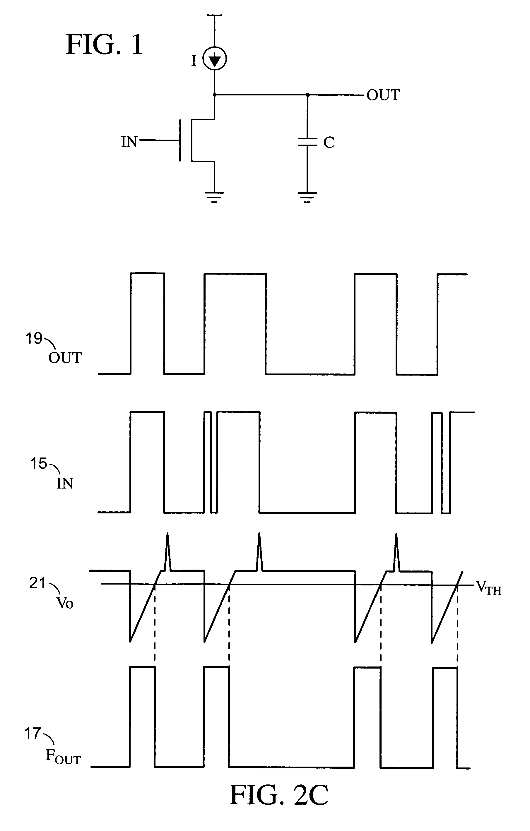
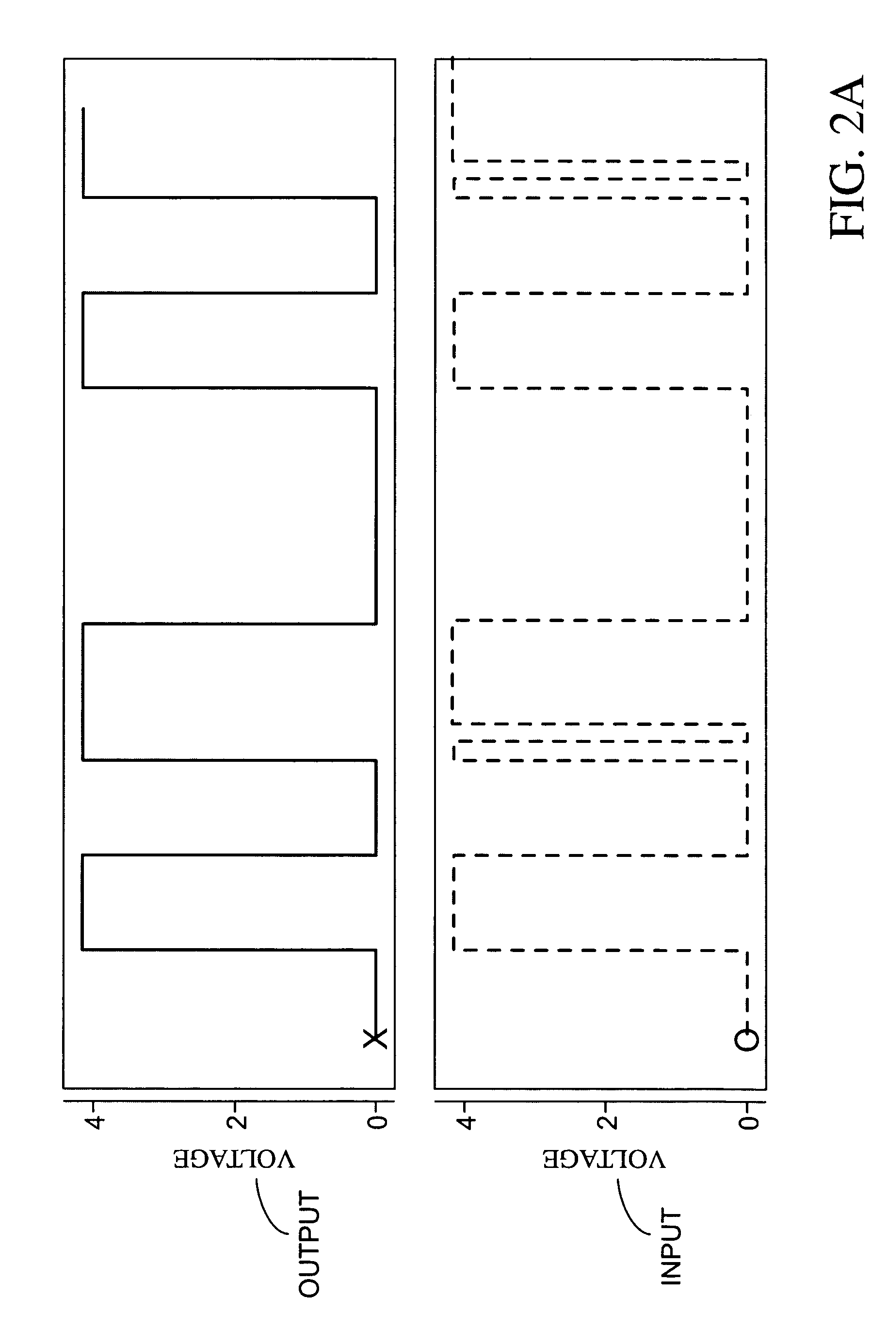
[0019]FIG. 2A shows input and desired output waveforms of the present invention. The input waveform IN shows a glitch or very short pulse that occurs after the rising transition of the input signal. Multiple short pulses can be present. The desired output OUT of the circuit is shown in the output waveform. The output signal OUT should transition to a logic high at the first transition of the input and stay high until the input signal transitions low, thereby ignoring any transitions after the initial high-going transition.

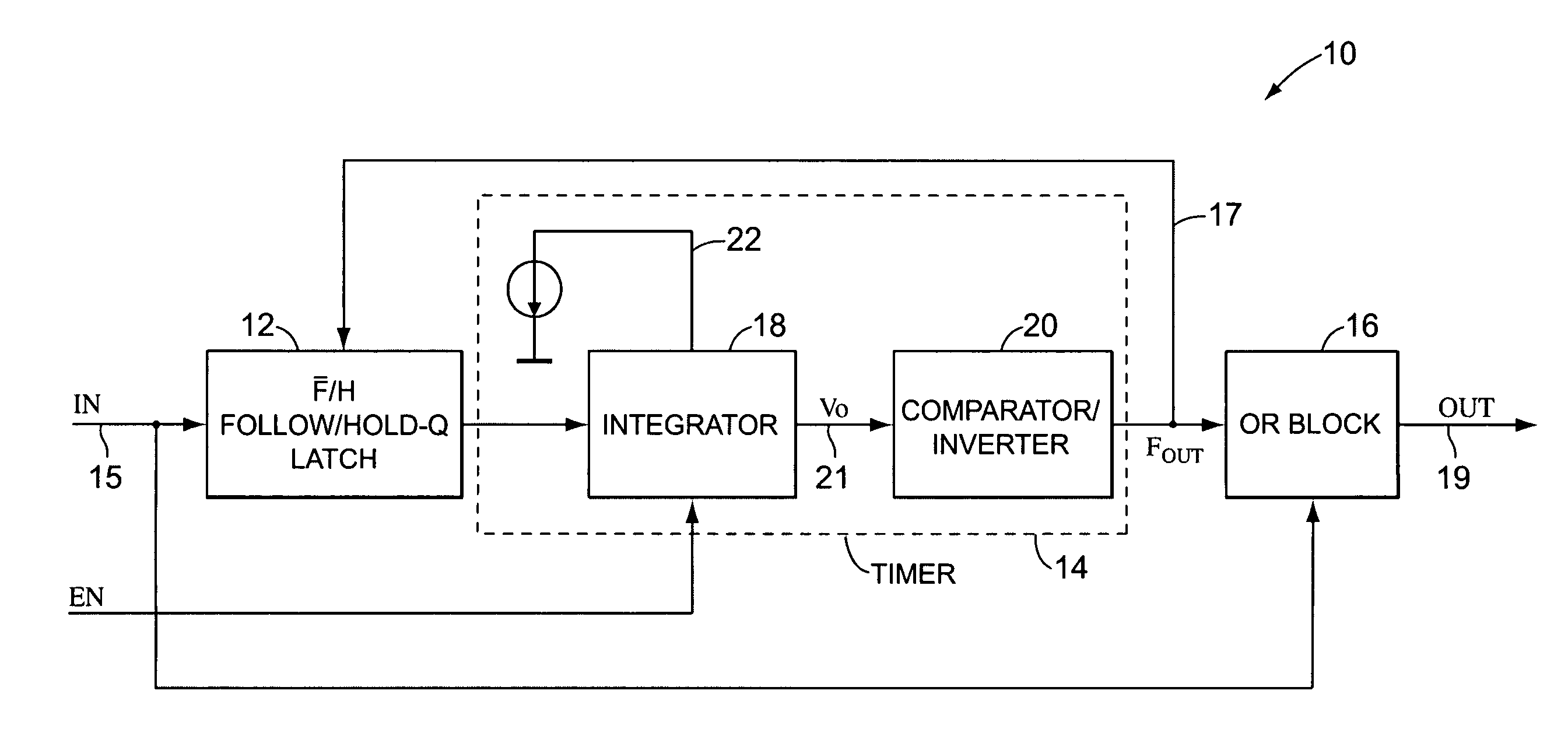
[0020]FIG. 2B shows a block diagram 10 of the present invention, which includes a follow / hold latch 12, a timer block 14, and a signal combining block (OR-block) 16. The follow / hold latch 12 is operative to follow the input signal IN 15 when a filter signal, Fout 17, is low and to hold the output when the filter signal is high. The timer block 14 creates the filter signal, Fout 17, which is fed back to control the follow / hold latch 12. The OR-block 16 combines the ...


PUM


Abstract

A system and method for filtering spurious transitions from a digital signal is disclosed. The system includes a latch, a timer, and a logic circuit. Upon a transition of the digital signal, the latch holds the digital signal to block any additional transitions and the timer, which is connected to the output of the latch, begins a timing operation that creates a filter pulse. The output of the timer is then combined with the digital signal to filter the spurious transitions that may occur after the transition of the signal. The timer is implemented as an integrator that generates a ramp signal using a stable current source and a comparator that trips when the ramp signal passes a threshold. Use of the integrator and comparator saves space and reduces the system's operating current compared to the conventional approach.

Description

FIELD OF THE INVENTION[0001]The present invention relates generally to noise filtering circuitry and more specifically to removal of noise in a digital circuit.DESCRIPTION OF THE RELATED ART[0002]In many mixed-modes, analog and digital, systems, for example in a switching voltage regulator, there often is full logic-level digital switching noise or ‘glitches’ due to substrate noise or switching noise. This unwanted digital noise is almost certain to cause erroneous system operation. FIG. 2A shows the input and output waveforms illustrating the problem. In the prior art, shown in FIG. 1, a switch, a large capacitor, and a current source providing a weak pull up are used to achieve this purpose. The disadvantages of the prior art are that it is difficult to control exactly how long to ignore the digital noise or glitches and there is no latch or flip-flop within this circuit that acts as a memory device to suppress multiple glitches that might occur.BRIEF SUMMARY OF THE INVENTION[0003...

Claims


Application Information

Patent Timeline
Patent Type & Authority Patents(United States)
IPC IPC(8): G06F17/10H03B1/00
CPCH03K5/1252
Inventor HO, DANIEL
Owner VIA TECH INC
Why Eureka
Try Eureka