Semiconductor device
- Summary
- Abstract
- Description
- Claims
- Application Information
AI Technical Summary
Benefits of technology
Problems solved by technology
Method used
Image
Examples
first embodiment
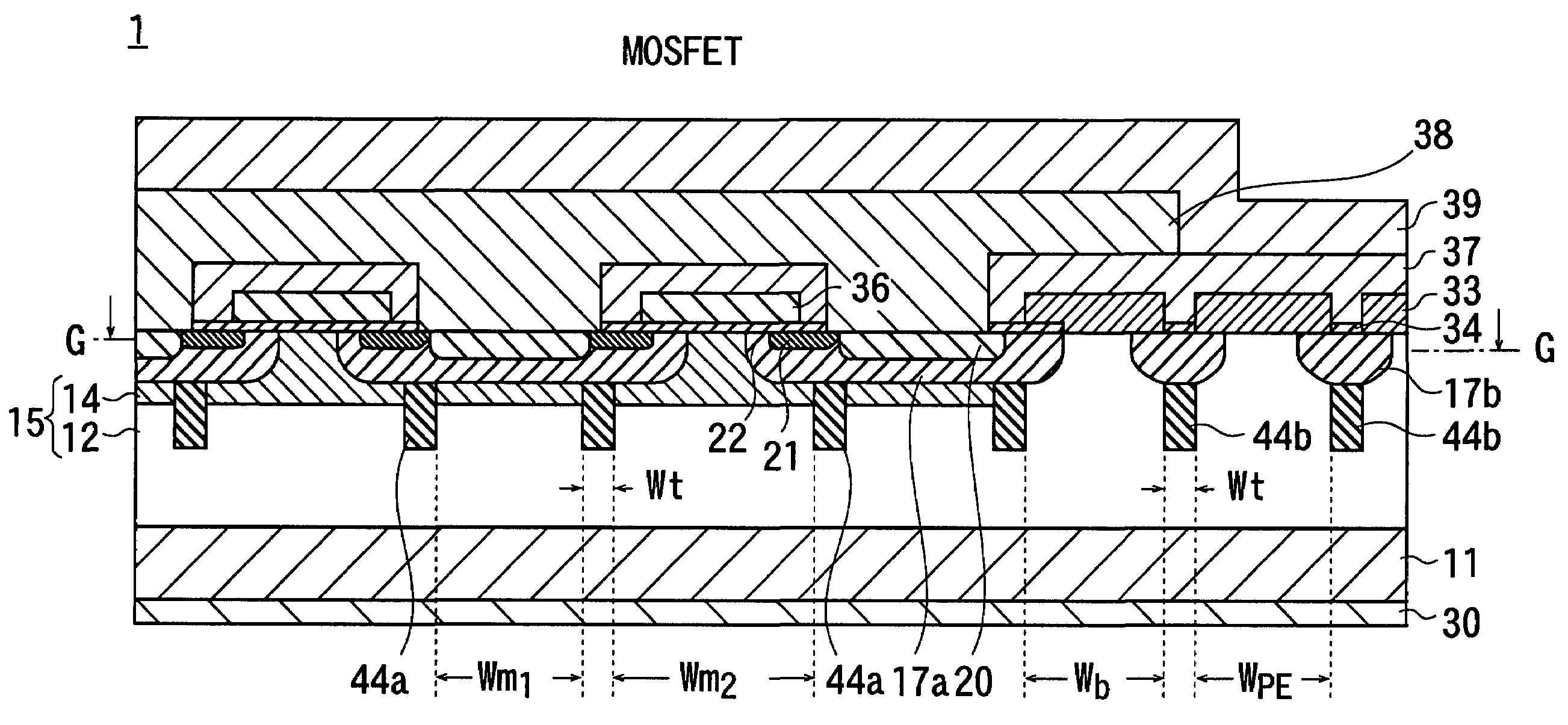
[0094]The structure of a semiconductor device according to the invention will be described. The reference numeral 1 in FIGS. 27 and 28 denotes a semiconductor device according to the invention.
[0095]A growth layer 12 of a first conductivity type is epitaxially grown on the surface of a wafer type semiconductor support layer 11 of the first conductivity type. A plurality of such semiconductor devices according to the invention are produced in a single wafer; and hereinafter, the internal structure of a single semiconductor device among them will be described with reference to the drawings.
[0096]A conductive layer 14 of the first conductivity type having a concentration higher than that of the growth layer 12 is formed at the inside surface of the growth layer 12 and in the center of the semiconductor device 1. The growth layer 12 and the conductive layer 14 form a resistance layer 15 that serves as the drain of a MOS transistor. Semiconductor devices without the conductive layer 14 a...
third embodiment
[0225]The reference numeral 3 in FIG. 34 denotes a Schottky junction type IGBT semiconductor device according to the invention.
[0226]In the semiconductor device 3, after the part corresponding to the semiconductor support layer 11 of the semiconductor device 1 according to the first embodiment is removed by polishing or the like, a metal film (such as, a chromium film forming a Schottky junction with the growth layer 12) is deposited on the surface of the growth layer 12 exposed by the polishing. The metal film forms a Schottky electrode film 56.
[0227]The Schottky junction has such a polarity that the junction is forward-biased in response to the conduction of the semiconductor device 3. When the Schottky junction is forward-biased, minority carriers are injected from the Schottky electrode film 56 into the growth layer 12, which lowers the conduction resistance.
fourth embodiment
[0228]The reference numeral 4 in FIG. 35 denotes the semiconductor device according to the invention, and a growth layer 12 of the first conductivity type is epitaxially grown on a support substrate 52 of the second conductivity type.
[0229]The semiconductor device 4 has an isolation diffusion region 53 formed by diffusion from the surface of the resistance layer 15 and its bottom reaches the support substrate 52.
[0230]The isolation diffusion region 53 has a ring shape and surrounds the active region in which the base diffusion region 17a is disposed.
[0231]Inside the region surrounded by the isolation diffusion region 53, a conductive layer 14 is formed, and in the vicinity of the inner surface of the conductive layer 14, a drain diffusion region 54 of the first conductivity type simultaneously formed with the source diffusion region 21 is provided. A drain electrode film 59 formed simultaneously with the source electrode film 38 and electrically insulated from the source electrode f...
PUM
 Abstract
Description
Claims
Application Information
 - R&D Engineer
- R&D Manager
- IP Professional
- Industry Leading Data Capabilities
- Powerful AI technology
- Patent DNA Extraction
Browse by: Latest US Patents, China's latest patents, Technical Efficacy Thesaurus, Application Domain, Technology Topic, Popular Technical Reports.
© 2024 PatSnap. All rights reserved.Legal|Privacy policy|Modern Slavery Act Transparency Statement|Sitemap|About US| Contact US: help@patsnap.com


