Inductor Q factor enhancement apparatus has bias circuit that is coupled to negative resistance generator for providing bias signal

a technology of bias signal and enhancement apparatus, which is applied in the field of circuits, can solve the problems of limited application of inductor, incompatible with the standard cmos manufacturing method, and significant common drawbacks of methods, and achieves the effects of enhancing the q factor of inductor, not affecting linearity, and low noise performance of inductor

Active Publication Date: 2009-09-01
REALTEK SEMICON CORP
View PDF6 Cites 4 Cited by
  • Summary
  • Abstract
  • Description
  • Claims
  • Application Information

AI Technical Summary

Benefits of technology

[0007]It is one of objectives of the claimed invention to provide an apparatus for enhancing the Q factor of an inductor. The apparatus is coupled to the inductor to eliminate power consumption of the inductor such that the Q factor of the inductor can be enhanced.
[0009]It is one of objectives of the claimed invention to provide an apparatus for enhancing the Q factor of an inductor. The apparatus does not affect the linearity and low noise performance of the inductor.

Problems solved by technology

This low Q factor often limits the application of an inductor.
However, these methods have a significant common drawback of being incompatible with the standard CMOS manufacturing methods.
However, the noise and linearity of an active circuit limits its application while being utilized in high-frequency and low-noise circuits.

Method used


Image

  • Inductor Q factor enhancement apparatus has bias circuit that is coupled to negative resistance generator for providing bias signal
  • Inductor Q factor enhancement apparatus has bias circuit that is coupled to negative resistance generator for providing bias signal
  • Inductor Q factor enhancement apparatus has bias circuit that is coupled to negative resistance generator for providing bias signal

Examples


Embodiment Construction

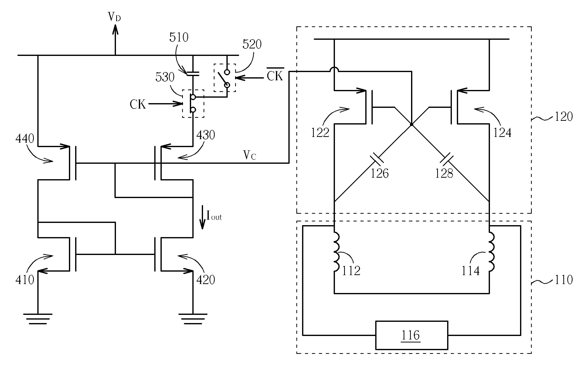
[0018]One method to enhance the Q factor of a chip inductor is reducing the power consumption of the chip inductor due to its parasitical resistor. The present invention adopts a negative resistance generator, which provides negative resistance, to compensate for the parasitical resistor of the chip inductor. Please refer to FIG. 1. FIG. 1 is the circuit configuration of the present invention illustrating a negative resistance generator 120 compensating for the parasitical resistors of inductors 112 and 114. The inductors 112 and 114 together with an operation circuit 116 construct an application circuit 110. The negative resistance generator 120 is coupled to the application circuit 110 to compensate for the parasitical resistors of the inductors 112 and 114. The negative resistance generator 120 comprises a pair of transistors 122 and 124, which couple to each other. In this embodiment, P-MOSFET's serve as exemplary devices for the transistors 122 and 124 for the sake of illustrat...


PUM

PropertyMeasurementUnit
resistance valueaaaaaaaaaa
negative resistanceaaaaaaaaaa
constant transconductance biasaaaaaaaaaa

Abstract

The present invention provides an apparatus for enhancing Q factor of an inductor. The apparatus includes a negative resistance generator coupled to the inductor for providing a negative resistance, and a bias circuit coupled to the negative resistance generator for biasing the negative resistance generator.

Description

BACKGROUND OF THE INVENTION[0001]1. Field of the Invention[0002]The present invention relates to a circuit, especially to a circuit capable of enhancing the Q factor of an inductor.[0003]2. Description of the Prior Art[0004]A typical inductor in an analog circuit is usually a planar inductor having a Q factor of approximately 3˜8. This low Q factor often limits the application of an inductor. For example, when an inductor is utilized as a load of an amplifier, the gain of the amplifier is proportional to the square of the inductor's Q factor. Therefore, a low Q factor implies a low gain. Moreover, in some narrow-band communication systems, an inductor with high Q factor is utilized for making a narrow-band resonant chamber capable of filtering out interfering signals. The 3 dB bandwidth of the resonant chamber is inversely proportional to the Q factor of the inductor. Therefore, an inductor with a higher Q factor leads to a narrower-band resonant chamber.[0005]Some methods for enhan...

Claims


Application Information

Patent Timeline
Patent Type & Authority Patents(United States)
IPC IPC(8): H03H11/00G05F1/14G06F7/64G06G7/12G06G7/18G06G7/19H04B1/10H03M1/12H03K5/00H03J3/20G11C27/02H01F29/04H03B1/00H03F1/02H03F3/45H03G3/12
CPCH03F1/565H03F3/345H03H11/52H03J3/20H03F2200/369
Inventor LIN, YING-YAOLIN, YING-HSI
Owner REALTEK SEMICON CORP
Why Eureka
Try Eureka