Nonvolatile semiconductor memory having a plurality of interconnect layers

a nonvolatile semiconductor and interconnect layer technology, applied in semiconductor devices, digital storage, instruments, etc., can solve the problems of reducing the performance of nand-type nonvolatile semiconductor memory, small and inability to detect change in bit line potential

Active Publication Date: 2009-09-15
KIOXIA CORP
View PDF8 Cites 18 Cited by
  • Summary
  • Abstract
  • Description
  • Claims
  • Application Information

AI Technical Summary

Problems solved by technology

As a result, a change in the bit line potential is small, and a change in the bit line potential may not be detected.
Accordingly, the cell source line charge / discharge time and recovery time for coupling noise occurs in a cell source line under the influence of other interconnects increases, reducing the performance of the NAND-type nonvolatile semiconductor memory.
As a result, the performance of the NAND-type nonvolatile semiconductor memory is reduced.
Accordingly, it is impossible to arrange cell source lines and / or cell well lines in the interconnect layer above the region where the memory cell transistors are arranged.
As a result, there is an undesirable change in the potential of the cell source lines arranged away from the cell source driver, and a change in the potential of the p-well region arranged away from the cell well driver.
As a result, a decrease in the interconnect resistance of the cell source lines and the interconnect resistance of the cell well lines cannot be sufficiently achieved.

Method used


Image

  • Nonvolatile semiconductor memory having a plurality of interconnect layers
  • Nonvolatile semiconductor memory having a plurality of interconnect layers
  • Nonvolatile semiconductor memory having a plurality of interconnect layers

Examples


first embodiment

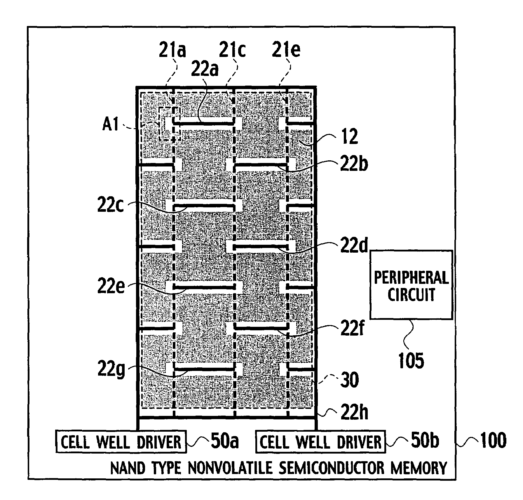
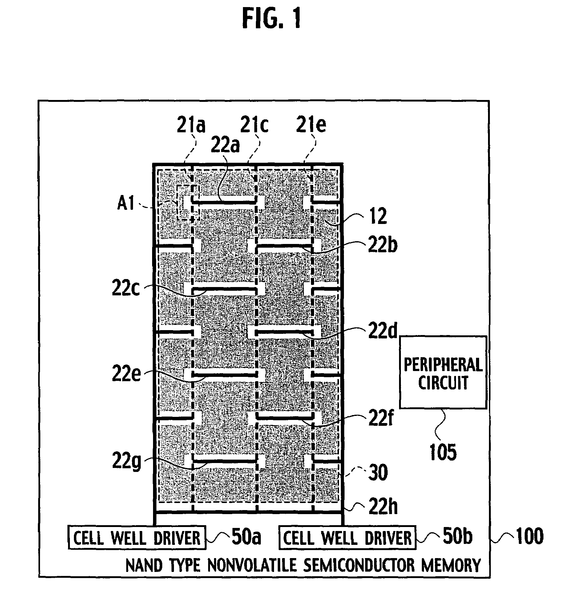
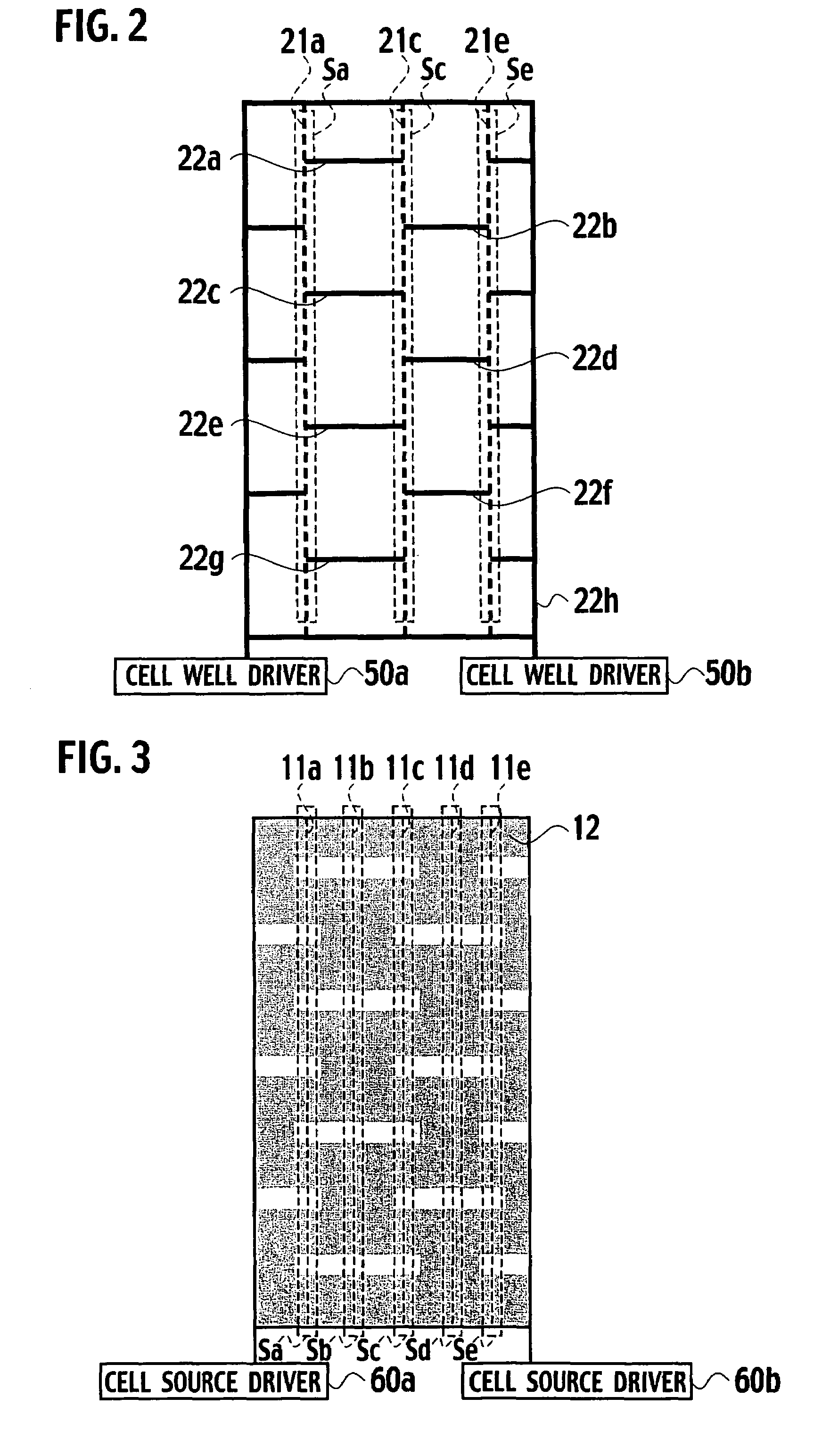
[0048]As shown in FIG. 1, a NAND-type nonvolatile semiconductor memory 100, according to the first embodiment of the present invention, includes a memory cell array 30, a plurality of first cell well lines 21a, 21c, and 21e, a plurality of second cell well lines 22a through 22h and a second cell source line 12. The memory cell columns, each including a plurality of vertically aligned memory cell transistors and select transistors that select the memory cell transistors, are horizontally aligned in the memory cell array 30. The first cell well lines 21a, 21c, and 21e are connected to well regions in which the memory cell columns are formed. The second cell well lines 22a through 22h are arranged in an interconnect layer above the first cell well lines 21a, 21c, and 21e. The second cell well lines 22a through 22h are connected to the first cell well lines 21a, 21c, and 21e so that the first cell well lines 21a, 21c, and 21e electrically connect to one another. The second cell source l...

second embodiment

[0080]As shown in FIG. 19, a NAND-type nonvolatile semiconductor memory, according to the second embodiment of the present invention, includes a memory cell array 30 in which horizontally aligned memory cell columns are arranged, each including vertically aligned memory cell transistors and select transistors configured to select the memory cell transistors, a plurality of first cell well lines 21a, 21c, and 21e are connected to well regions, respectively, in which a plurality of memory cell columns are formed, a plurality of first cell source lines, which are connected to the source terminals of the respective select transistors in the plurality of memory cell columns, a second cell well line 23, which is arranged in an interconnect layer above the first cell well lines 21a, 21c, and 21e and electrically is connected to the first cell well lines 21a, 21c, and 21e to one another, and a second cell source line 13, which is arranged in an interconnect layer in which the second cell we...

third embodiment

[0091]As shown in FIG. 27, a NAND-type nonvolatile semiconductor memory according to the third embodiment of the present invention includes vias 121i through 121l on a shunt region Sa on which vias 221i through 221m connect a second cell well line 23 arranged in the second interconnect layer and first cell well lines 21i through 21m arranged in the first interconnect layer. The vias 121i through 121l connect a second cell source line 13 arranged in a second interconnect layer and first cell source lines 11i through 11l arranged in a first interconnect layer.

[0092]As shown in FIG. 27, the vias 221i through 221m and 121i through 121l are linearly arranged along the memory cell column length. FIG. 27 shows only the vias 221i through 221m and 121i through 121l arranged above the shunt region Sa; however, vias which connect the second cell source line 13 and cell source lines arranged in the first interconnect layer are arranged above the shunt regions Sc and Se, as well as the shunt reg...


PUM


Abstract

A nonvolatile semiconductor memory includes a memory cell array including horizontally aligned memory cell columns, each including vertically arranged memory cell transistors and select transistors selecting the memory cell transistors; first cell well lines connecting well regions in which the memory cell columns are formed; second cell well lines arranged in an interconnect layer above the first cell well lines and connecting the first cell well lines to one another electrically; and a cell source line connecting source terminals of the select transistors in each memory cell column.

Description

CROSS REFERENCE TO RELATED APPLICATIONS AND INCORPORATION BY REFERENCE[0001]This application is based upon and claims the benefit of priority from prior Japanese Patent Application P2005-029280 filed on Feb. 4, 2005 and prior Japanese Patent Application P2006-011646 filed on Jan. 19, 2006; the entire contents of which are incorporated by reference herein.BACKGROUND OF THE INVENTION[0002]1. Field of the Invention[0003]The present invention relates to a semiconductor memory, particularly to a nonvolatile semiconductor memory having a plurality of interconnect layers.[0004]2. Description of the Related Art[0005]A plurality of memory cell transistors are arranged in a matrix on a memory cell array region of a nonvolatile semiconductor memory. In a nonvolatile semiconductor memory, a determination of whether each of memory cell transistors stays either in a logic ‘1’ state or a logic ‘0’ state is based on a threshold voltage varying in relation to the amount of charge accumulated in each...

Claims


Application Information

Patent Timeline
Patent Type & Authority Patents(United States)
IPC IPC(8): G11C16/22
CPCG11C16/0483H01L27/11524H01L27/11521H01L27/115H10B69/00H10B41/30H10B41/35
Inventor ABE, TAKUMIFUKUDA, KOICHIMAEJIMA, HIROSHI
Owner KIOXIA CORP
Why Eureka
Try Eureka