Nanoparticle electroluminescence and method of manufacturing the same

a technology of nanoparticles and electroluminescence, which is applied in the direction of cleaning equipment, natural mineral layered products, applications, etc., can solve the problems of affecting the luminescence efficiency and luminescence characteristics dangling bonds or vacancy etc. may exist on the surface of si fine particles, so as to achieve excellent light emission and improve luminescence efficiency

Active Publication Date: 2009-09-22
SAMSUNG ELECTRONICS CO LTD
View PDF4 Cites 34 Cited by
  • Summary
  • Abstract
  • Description
  • Claims
  • Application Information

AI Technical Summary

Benefits of technology

[0008]The present disclosure provides a nanoparticle electroluminescence device having excellent light emission and an improved luminescence efficiency, and a method of manufacturing the same.
[0011]According to the present disclosure having the above structure, the nanoparticle electroluminescence device having excellent light emission and an improved luminescence efficiency can be obtained.

Problems solved by technology

However, defects such as dangling bonds or vacancy etc. may exist on the surface of the Si fine particles.
These defects may badly affect luminescence efficiency and luminescence characteristics of Si fine particles.

Method used


Image

  • Nanoparticle electroluminescence and method of manufacturing the same
  • Nanoparticle electroluminescence and method of manufacturing the same
  • Nanoparticle electroluminescence and method of manufacturing the same

Examples


Embodiment Construction

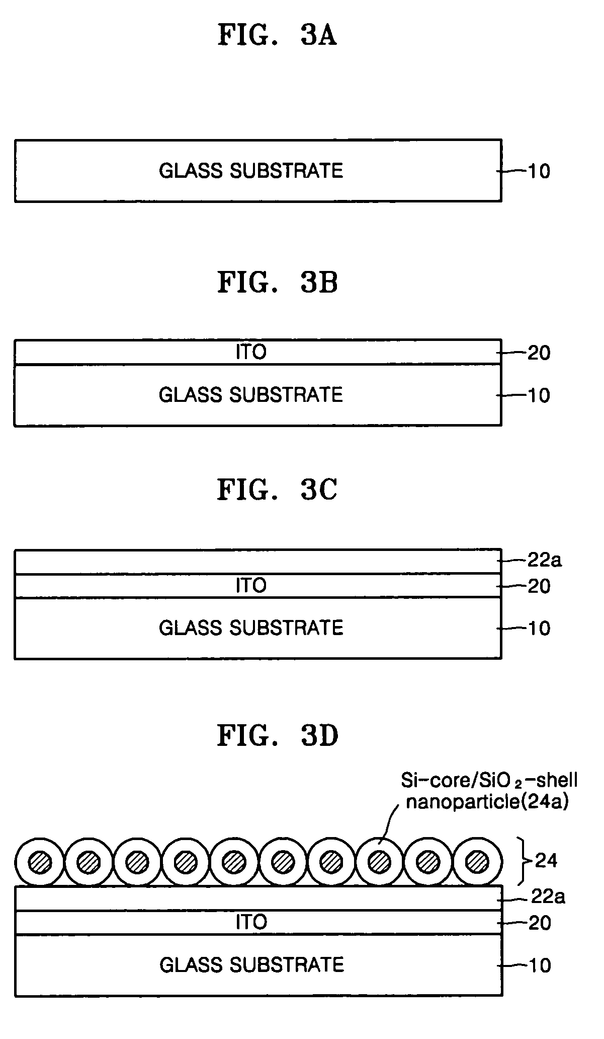
[0017]Hereinafter, the present invention will be described in detail by explaining exemplary embodiments of the invention with reference to the attached drawings. In the drawings, the thicknesses of layers and regions are exaggerated for clarity.

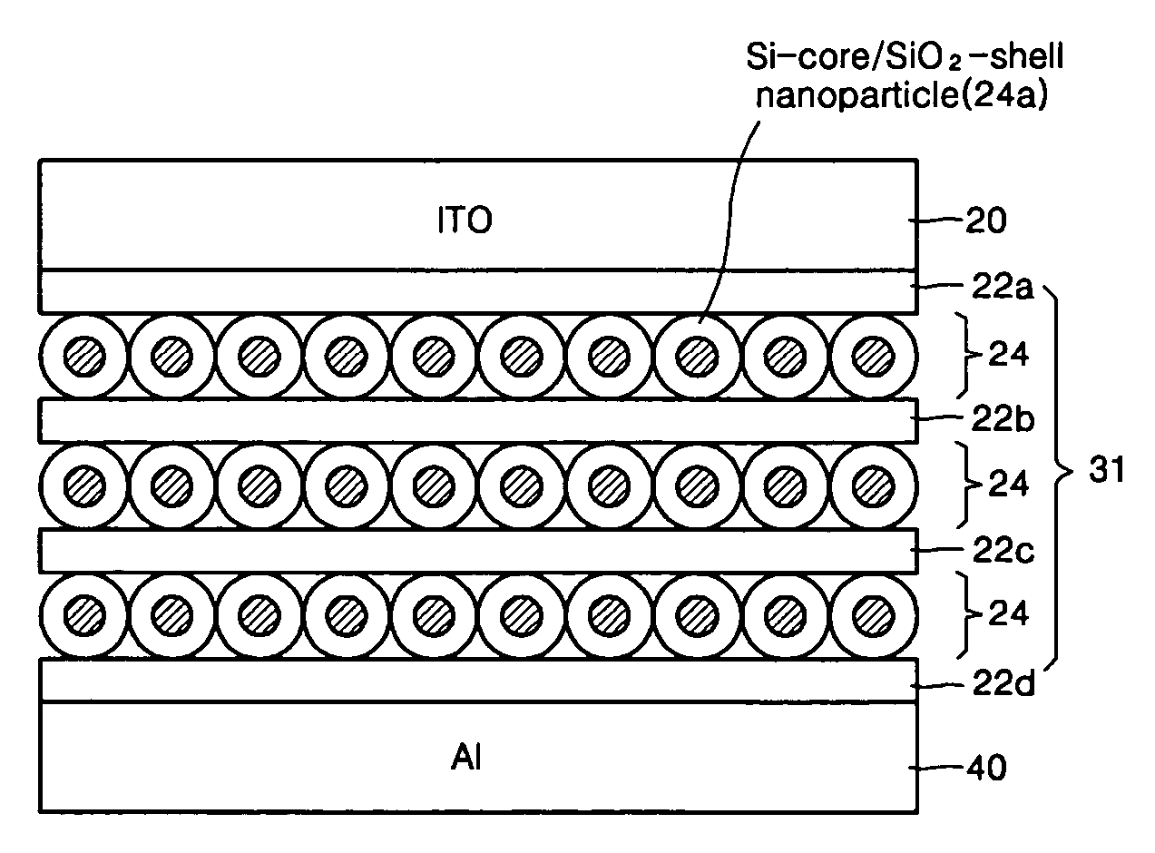
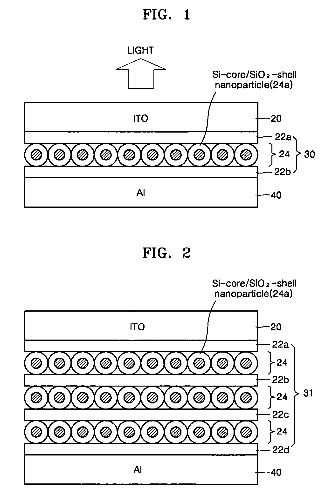
[0018]FIG. 1 is a schematic cross-sectional view of a nanoparticle eletroluminescence device according to an embodiment of the present invention. Referring to FIG. 1, the nanoparticle electroluminescence device according to the present disclosure includes a front electrode 20, a rear electrode 40, and an emitting layer (EML) 30 interposed between the front electrode 20 and the rear electrode 40.

[0019]The emitting layer (EML) 30 is an area in which recombination of electrons and holes supplied from both electrodes 20 and 40 is performed and luminescence is produced. Here, the EML 30 includes nanoparticles 24a having a core / shell structure comprising a core formed of silicon and a shell formed of silicon oxide (SiO2) or silicon nitride (Si3N4)...


PUM

PropertyMeasurementUnit
diameteraaaaaaaaaa
diameteraaaaaaaaaa
thicknessaaaaaaaaaa

Abstract

The nanoparticle electroluminescence device includes: a front electrode formed of a transparent conductive material; a rear electrode formed of a conductive material; and an emitting layer interposed between the front electrode and the rear electrode and comprising a plurality of nanoparticles having a core / shell structure comprising a core formed of silicon and a shell formed of silicon oxide or silicon nitride on the surface of the core.

Description

CROSS-REFERENCE TO RELATED PATENT APPLICATIONS[0001]Priority is claimed to Korean Patent Application No. 10-2005-0015574, filed on Feb. 24, 2005, in the Korean Intellectual Property Office, the disclosure of which incorporated herein in its entirety by reference.BACKGROUND OF THE INVENTION[0002]1. Field of the Disclosure The present disclosure relates to an electroluminescence device and a method of manufacturing the same, and more particularly, to a nanoparticle electroluminescence device having excellent light emission and an improved luminescence efficiency, and a method of manufacturing the same.[0003]2. Description of the Related Art[0004]Electroluminescence (EL) devices are devices which emit light by electrical excitation. For example, when electric energy is supplied to electrons in a low energy level and the electrons move to a higher energy level when the electric energy is cut off, the electrons return to the low energy level and light of predetermined wavelength may be g...

Claims


Application Information

Patent Timeline
Patent Type & Authority Patents(United States)
IPC IPC(8): H01L33/00H01L33/34H01L33/42
CPCC09K11/02C09K11/59C09K11/592H05B33/14Y10T428/259Y10S977/95Y10S977/952A47L9/1608A47L9/1683
Inventor KHANG, YOON-HOLEE, EUN-HYULEE, KYO-YEOLLEE, JOO-HYUNIM, SEONG-IL
Owner SAMSUNG ELECTRONICS CO LTD
Why Eureka
Try Eureka