Substrate of emitting device and emitting device using the same

a technology of emitting device and substrate, which is applied in the direction of solid-state devices, electric lighting sources, electric light sources, etc., can solve the problems of low affecting the efficiency of light emitting, and the upper limit of light-emitting probability, etc., to achieve good light-emitting efficiency

Active Publication Date: 2005-03-10
SAMSUNG DISPLAY CO LTD
View PDF17 Cites 25 Cited by
  • Summary
  • Abstract
  • Description
  • Claims
  • Application Information

AI Technical Summary

Benefits of technology

[0024] Therefore, in view of the foregoing, an objective of the present invention is to provide a substrate for a light-emitting device and light-emitting device using the same, in which the problems of the prior arts are solved and the light emitting efficiency is good.

Problems solved by technology

However, in the organic EL device, the upper limit of a light-emitting probability exists because of restriction on a singlet formation probability rather than dependency on the spin statistics during recombination of carriers.
In the organic EL device in which the light-emitting is strictly restricted, the low efficiency of the light emitting incurs decrease of the energy conversion efficiency considered to be fatal.
Particularly, in the organic EL device, because the thickness of the emitting layer is less than several microns, it is difficult not only to form the reflection mirror, which has a tapered surface on the lateral surface of the device, even by use of the current technique, but also to avoid sharp increase of cost.
However, since the light is reflected at the interface between the anode and the low refractive index layer, improvement of the light emitting efficiency is still considered to be insufficient.
Further, in the case of using the polished silica aerogel layer in order to obtain the very low refractive index layer, a mechanical strength of the layer is very weak.
Further, a short of the electrode caused by surface unevenness of the polished layer is generated, so that portions where the light is not emitted (dark spots) are generated.
Light extracting technique effective for the organic EL device does not still reach a satisfactory level.
For this reason, when the technique of the document is employed to the light-emitting device for a white color, a quantity of light emitted outside the substrate is greatly changed by the wavelength, so that deterioration of white balance becomes problematic.
As a result, the light-emitting device is vulnerable to an error in its performance.

Method used


Image

  • Substrate of emitting device and emitting device using the same
  • Substrate of emitting device and emitting device using the same
  • Substrate of emitting device and emitting device using the same

Examples


first embodiment

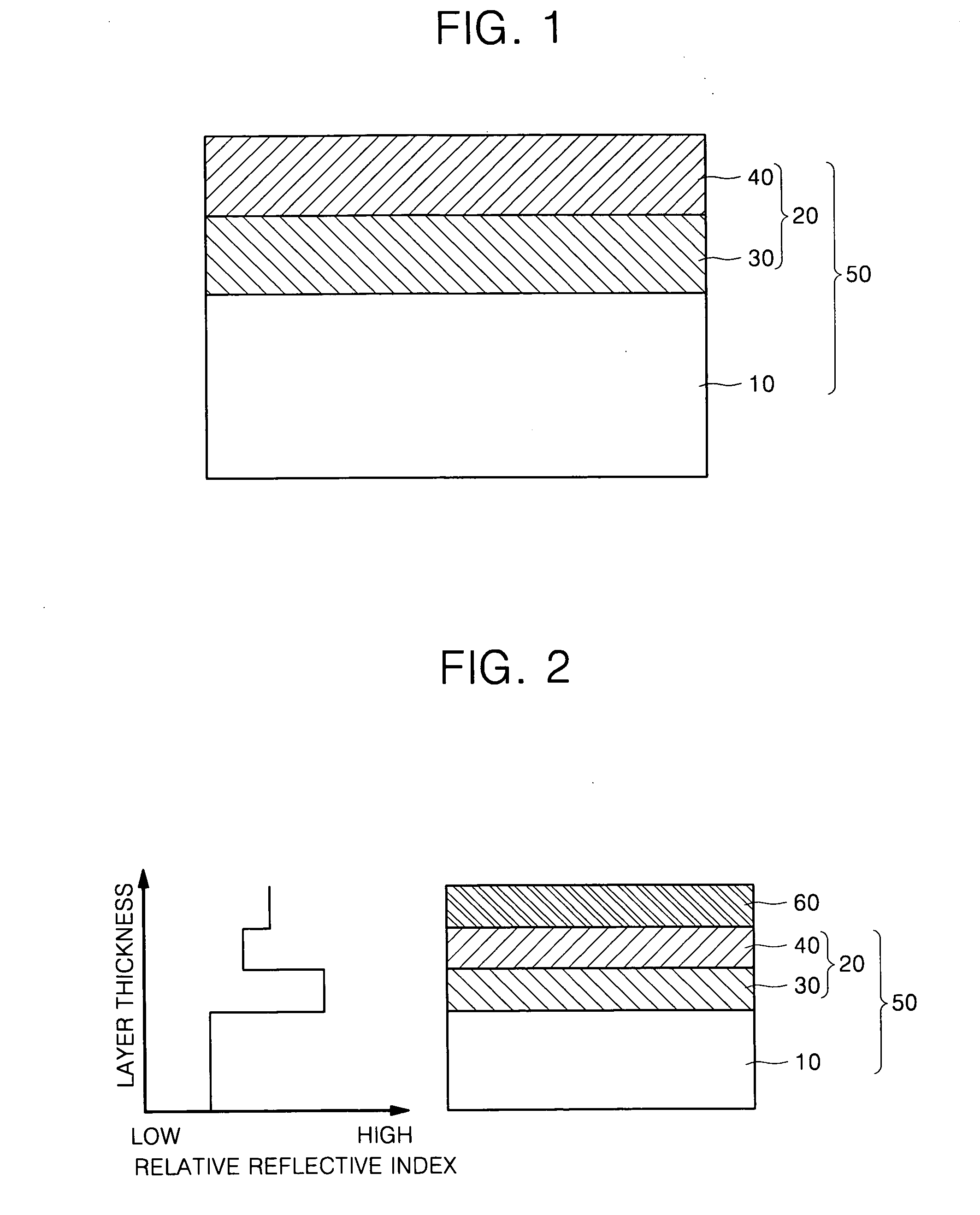
[0064]FIG. 1 is an exemplary cross-sectional view of a substrate for a light-emitting device according to the present embodiment. Specifically, a substrate 50 for the light-emitting device of the present invention is provided with an optical control layer 20 on one surface of a light transparent substrate 10. The optical control layer 20 is composed of a first layer 30 which has a refractive index higher than that of the light transparent substrate 10, and a second layer 40 which has a refractive index lower than that of the first layer 30, and has a structure where these two layers are layered from the light transparent substrate 10 in that order.

[0065] This substrate for the light-emitting device is used as a substrate of a light-emitting device by mounting an emitting region on an upper portion of the optical control layer 20. The optical control layer 20 converts a wave front of a spherical wave form of emission introduced from the upper portion thereof into that of a plane wav...

second embodiment

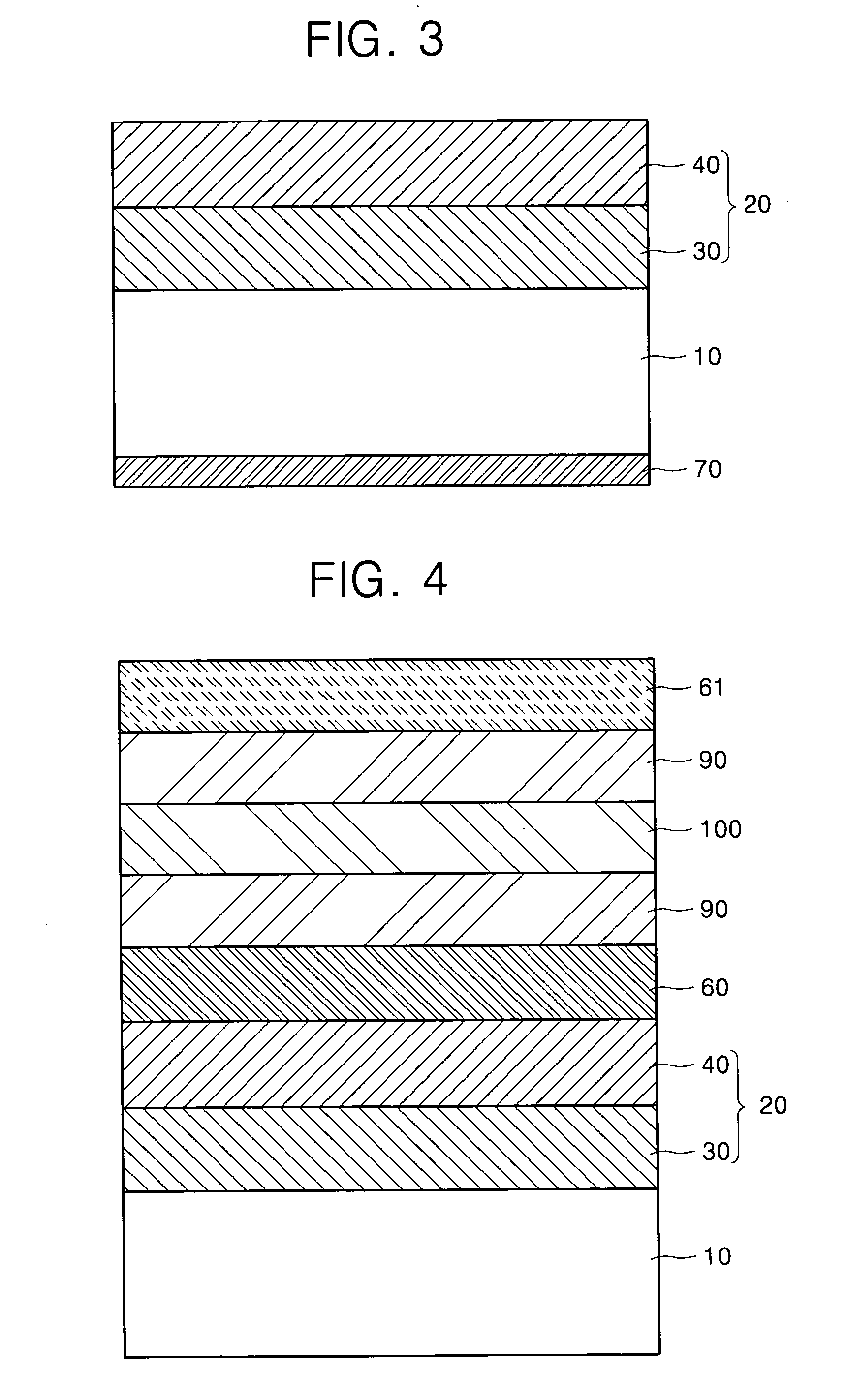
[0090]FIG. 4 shows one example of an exemplary cross-sectional view of an inorganic EL device using a substrate for a light-emitting device in accordance to the present embodiment. The light transparent substrate 10 has one surface provided with the optical control layer 20 on which the electrode layer 60, an insulating layer 90, an inorganic emitting layer 100, the insulating layer 90 and the electrode layer 60 are sequentially provided in that order.

[0091] The optical control layer 20 is composed of the first layer 30 having the refractive index higher than that of the light transparent substrate 10 and the second layer 40 having the refractive index higher than that of the first layer 30, both of which are sequentially provided from the light transparent substrate 10. The first layer 30 is disposed on the light transparent substrate 10. And, either a configuration of the inorganic EL device or its material may be arbitrarily selected from the well-known ones.

[0092] According to...

third embodiment

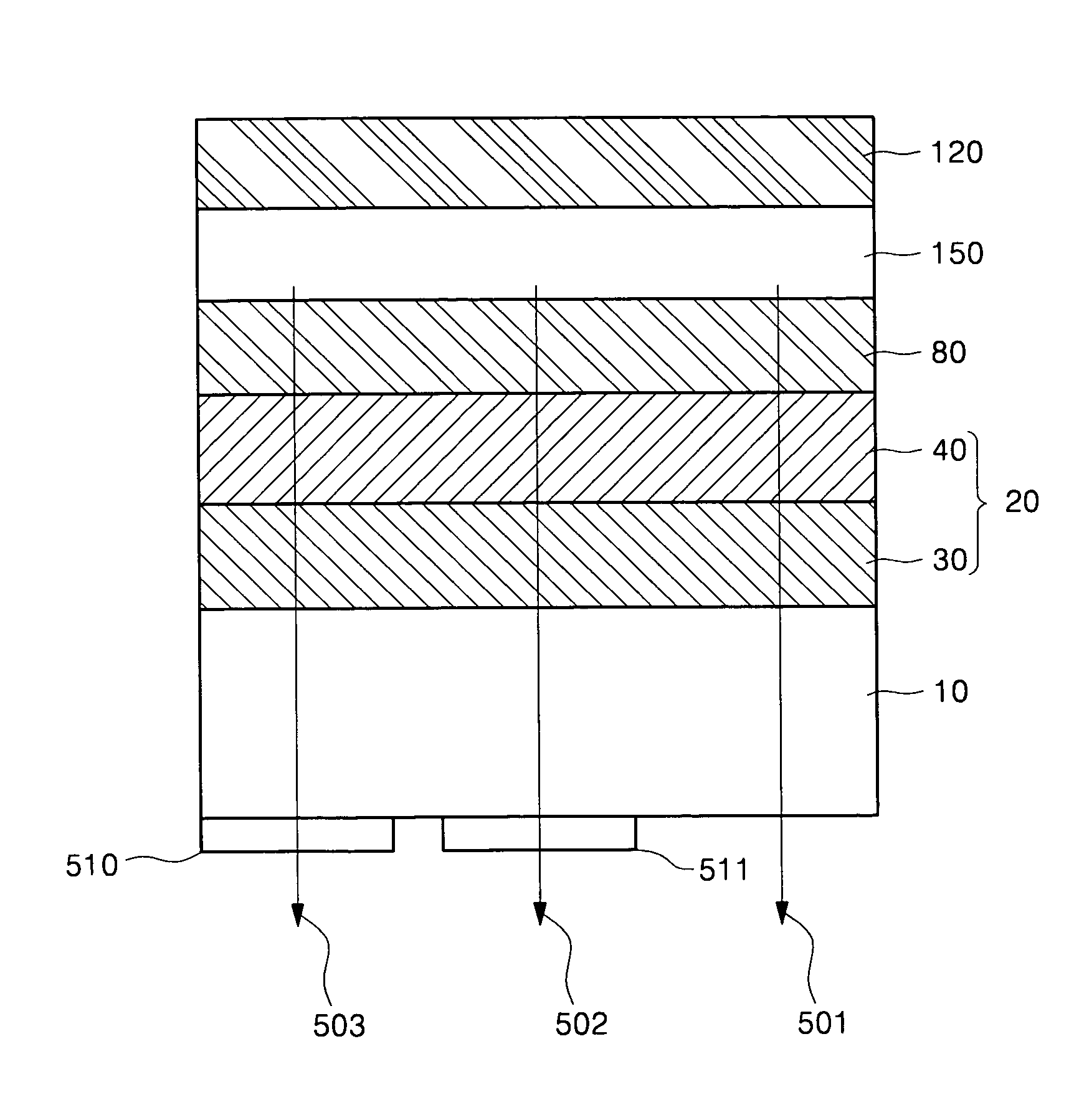
[0093] This embodiment shows an example where the substrate for the light-emitting device described in the first embodiment is applied to an organic EL device. FIG. 5 is an example of a schematic cross-sectional view showing a structure of an organic EL device in accordance with this embodiment. In this embodiment, the substrate for the light-emitting device is sequentially provided with a positive electrode (anode) 80, an emitting layer 130 and a negative electrode (cathode) 120.

[0094]FIG. 6 is an example of an exemplary cross-sectional view showing another structure of an organic EL device related to this embodiment. In this embodiment, the substrate for the light-emitting device is sequentially provided with the positive electrode 80, a hole transporting layer 140, the emitting layer 130 and the negative electrode 120. In addition, other structures may be enumerated, for example a structure composed of positive electrode / hole transporting layer / emitting layer / electron transporti...


PUM


Abstract

Provided is a substrate for a light-emitting device having good light emitting efficiency and light-emitting device using the substrate. A light transparent substrate 10 is layered with a first layer 30 having a refractive index higher than that of the light transparent substrate 10 and a s second layer 40 having a refractive index lower than that of the first layer. The refractive index of the first layer 30 is set to be 1.35 times as high as that of the second layer 40. With this layer structure, in an emitting layer of the light-emitting device, a wave front of a spherical wave form exited from a point light source in the front direction is converted into that of a plane wave form, and exited outside the substrate at a high efficiency.

Description

CROSS-REFERENCE TO RELATED APPLICATION [0001] This application claims the benefit of Japanese Patent Application No. 2003-319106, filed Sep. 10, 2003, the disclosure of which is hereby incorporated herein by reference in its entirety. BACKGROUND OF THE INVENTION [0002] 1. Field of the Invention [0003] The present invention relates to a substrate for a light-emitting device and an optical device using the same. [0004] 2. Description of the Related Art [0005] An organic electroluminescence (EL) device is a spontaneous emitting display device employing a principle that fluorescent material emits light in response to recombination energy of holes injected from an anode and an electrons injected from a cathode when an electric field is applied. After a layered low-voltage driven organic EL device is reported, studies on the organic EL device using an organic material as a constituent material have been briskly performed. [0006] Tang et al. teaches that an emitting layer is formed of a tr...

Claims


Application Information

Patent Timeline
Patent Type & Authority Applications(United States)
IPC IPC(8): H01L51/40H01L51/50H05B33/02H01L51/52H05B33/12H05B33/14H05B33/22H05B33/26
CPCH01L51/5262H10K50/85H05B33/22
Inventor GOTOH, TOMOHISATAKEWAKI, NORIKOTSUGE, HISANAOKAMIJO, ATSUSHITOGUCHI, SATORU
Owner SAMSUNG DISPLAY CO LTD
Why Eureka
Try Eureka