Delay locked loop circuit

a technology of locking loop and loop, applied in the direction of pulse rate multipliers/dividers, computations using non-denominational number representations, pulse automatic control, etc., can solve the problem of difficulty in exactly transmitting/receiving data to/from the dram, and achieve the effect of preventing a locking failur

Active Publication Date: 2009-10-20
SK HYNIX INC
View PDF15 Cites 10 Cited by
  • Summary
  • Abstract
  • Description
  • Claims
  • Application Information

AI Technical Summary

Benefits of technology

[0024]It is, therefore, an object of the present invention to provide a delay locked loop (DLL) circuit of a semiconductor memory device for preventing a locking failure occurring from a change in a circumstance of the semiconductor device, such as an external temperature, in a power down mode for a relatively long time.

Problems solved by technology

As a result, it is difficult to exactly transmit / receive data to / from the DRAM because phase of the external clock signal is different from that of the DLL clock signal DLL_CLK of the DLL circuit.

Method used


Image

  • Delay locked loop circuit
  • Delay locked loop circuit
  • Delay locked loop circuit

Examples


first embodiment

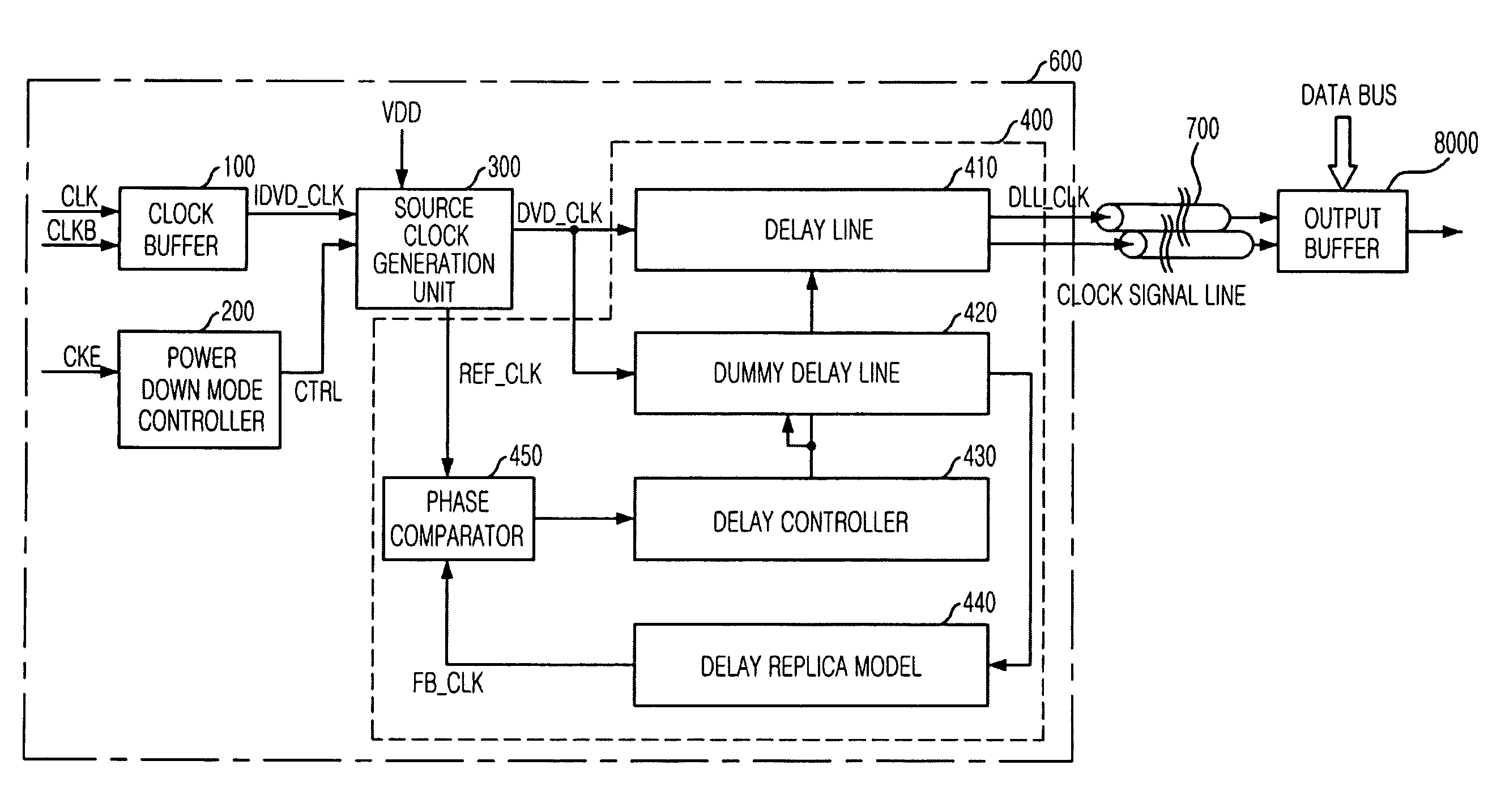
[0053]FIG. 5 is a block diagram of the source clock generation unit 300 shown in FIG. 4 in accordance with the present invention; and FIGS. 6A and 6B are detailed circuit diagrams of a second clock divider shown in FIG. 5.

[0054]As shown, the source clock generation unit 300 in accordance with the first embodiment of the present invention includes first and second clock dividers 310 and 320, a selection unit 330, an operational logic unit 340, and a reference clock generation unit 350.

[0055]The first clock divider 310 generates a first division clock signal CLK_D1 to set a duration of the phase update operation in the normal mode by dividing the internal clock signal IDVD_CLK.

[0056]The second clock divider 320 generates a second division clock signal CLK_D2 to set a duration of the phase update operation in the power down mode by dividing the first division clock signal CLK_D1.

[0057]The selection unit 330 selects one of the first and second division clock signals CLK_D1 and CLK_D2 ba...

second embodiment

[0076]FIG. 10 is a block diagram showing the source clock generation unit shown 300 in FIG. 4 in accordance with the present invention; and FIGS. 11A and 11B are detailed circuit diagrams of a clock conversion unit of the source clock generation unit 300 shown in FIG. 10.

[0077]Referring to FIG. 10, the source clock generation unit 300 in accordance with the second embodiment of the present invention includes a selection unit 330, an operational logic unit 340, a reference clock generation unit 350, a clock conversion unit 360 and a clock divider 370.

[0078]The clock divider 370 generates a first conversion clock signal CLK_T1 to set a duration of the phase update operation in the normal mode by dividing the internal clock signal IDVD_CLK.

[0079]The clock conversion unit 360 generates a second conversion clock signal CLK_T2 to set a duration of the phase update operation in the power down mode by converting the first conversion clock signal CLK_T1.

[0080]The selection unit 330 selects o...


PUM


Abstract

A DLL of a memory device having a normal mode and a power down mode includes a clock buffer for buffering an external clock signal to output an internal clock signal. A power down mode controller generates a power down mode control signal to define the normal mode or the power down mode in response to a clock enable signal. A source clock generation unit receives the internal clock signal to generate a DLL source clock signal under the control of the power down mode control signal. A phase update unit performs a phase update operation based on the DLL source clock signal to output a DLL clock signal.

Description

FIELD OF THE INVENTION[0001]The present invention relates to a delay locked loop (DLL) circuit of a synchronous DRAM; and, more particularly, to a DLL circuit for performing a stable operation in a power down mode for low power operation of a semiconductor device.DESCRIPTION OF RELATED ARTS[0002]A synchronous semiconductor memory device such as a double data rate synchronous DRAM (DDR SDRAM) performs data transmission with external devices using an internal clock signal locked in synchronization with an external clock signal input from an external device such as a memory controller. Time synchronization between a reference clock signal and data is important for stably transmitting the data between a memory device and a memory controller. In order to transmit the data stably, the data should be positioned accurately at an edge or a center of the clock by compensating for delay time which occurs inevitably by virtue of the time difference between the data transmission of each element ...

Claims


Application Information

Patent Timeline
Patent Type & Authority Patents(United States)
IPC IPC(8): H03L7/06
CPCG06F7/68H03L7/0814H03L7/0805H03L7/0816
Inventor CHOI, HOONLEE, JAE-JIN
Owner SK HYNIX INC
Why Eureka
Try Eureka