Backplanes for display applications, and components for use therein

a backplane and display technology, applied in the field of backplanes for electrooptic (electronic) displays, can solve the problems of preventing their widespread use, inability to transmit, and inability to be bistable, and achieve the effect of simple processing steps and reduced manufacturing costs

Inactive Publication Date: 2009-10-20
E INK CORPORATION
View PDF164 Cites 157 Cited by
  • Summary
  • Abstract
  • Description
  • Claims
  • Application Information

AI Technical Summary

Benefits of technology

[0035]As already mentioned, one aspect of this invention relates to registration-tolerant transistor (especially TFT) designs. The transistors are particularly useful for addressing display media in a display device, and in some embodiments can provide relatively low pixel-to-pixel variations in gate-pixel capacitance.
[0036]Accordingly, in one aspect this invention provides a transistor comprising a source electrode, a drain electrode spaced from the source electrode by a channel, a semiconductor layer extending across the channel, and a gate electrode disposed adjacent the channel such that application of a voltage to the gate electrode will vary the conductivity of the semiconductor layer extending across the channel. The gate electrode has a first gate electrode edge and a second gate electrode edge spaced from the first gate electrode edge. The drain electrode has a first drain electrode edge portion which overlaps the first gate electrode edge to define a first overlap area, and also has a second drain electrode edge portion which overlaps the second gate electrode edge to define a second overlap area, such that translation of the gate electrode relative to the drain electrode in a direction which increases the first overlap area will decrease the second overlap area, or vice versa.
[0061]Preferred embodiments of the two processes of the present invention can produce displays addressed by n / i / n (i.e., n-type / intrinsic / n-type) or i / n / i a-Si diode arrays and with a resolution that is comparable to displays addressed by TFT arrays. The diode array can be manufactured via low-cost methods having fewer, simpler processing steps than conventional processes for forming such diode arrays.
[0062]In another aspect, this invention provides a backplane for an electro-optic display. This backplane comprises a source line, a transistor and a pixel electrode connected to the source line via the transistor. The pixel electrode extends over part of the source line to form an overlap area. The backplane also comprises a conductive portion disposed between the source line and the pixel electrode, this conductive portion reducing the source line / pixel electrode capacitance.

Problems solved by technology

Nevertheless, problems with the long-term image quality of these displays have prevented their widespread usage.
For example, particles that make up electrophoretic displays tend to settle, resulting in inadequate service-life for these displays.
Liquid crystals, including polymer-dispersed liquid crystals, are, of course, also electro-optic media, but are typically not bistable and operate in a transmissive mode.
Fabrication processes, however, can result in significant cost.
The voltage biases can cause errors in the optical states of pixels, as well as degrade the electro-optic medium.
This technique, however, can cause a large gate-pixel capacitance.
A large gate-pixel capacitance is undesirable because it can create a need for a large compensation in one of the select line voltage levels.
Moreover, existing addressing structures can produce unintended bias voltages, for example, due to pixel-to-pixel variations in gate-pixel capacitance.
Such voltages can produce a detrimental effect on certain electro-optic media, particularly when present for extended periods of time.
These field lines cause undesired optical shifts that are typically hidden from an observer by a light blocking patterned mask on the viewing surface of the display.
The field shielded design does, however, result in the source and select lines have a relatively large capacitative coupling to the pixel electrodes.
Consequently, the pixel electrodes experience significant voltage shifts whenever an underlying source or select line shifts in voltage, and these voltage shifts can induce unwanted optical transitions in the electro-optic medium layer.
However, both approaches have disadvantages; larger storage capacitors require larger transistors and increase the power consumption of the display and parasitic voltages therein, and thinner source and select lines produce larger resistive voltage drops and increase the chance of line breaks.
Thus, there is no universal way to compensate for pixel voltage shifts caused by capacitative coupling to source lines in standard backplane designs.

Method used


Image

  • Backplanes for display applications, and components for use therein
  • Backplanes for display applications, and components for use therein
  • Backplanes for display applications, and components for use therein

Examples


Embodiment Construction

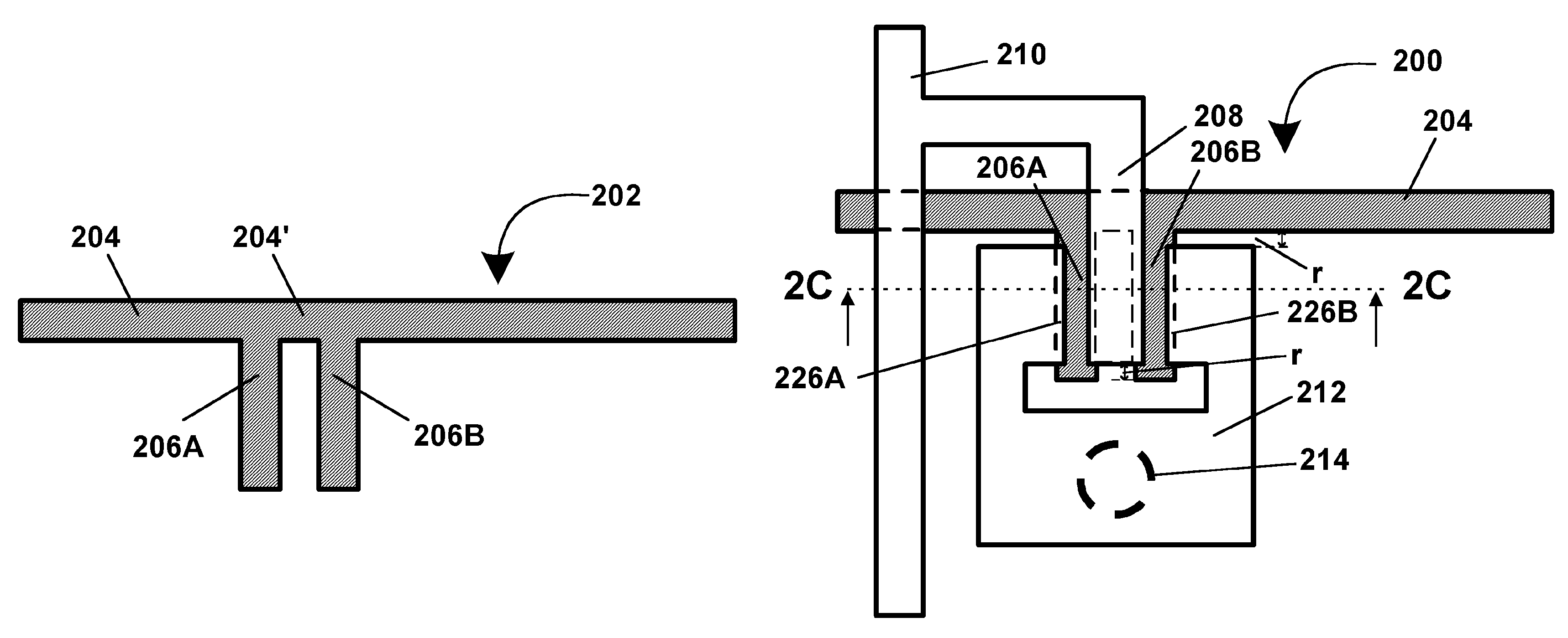
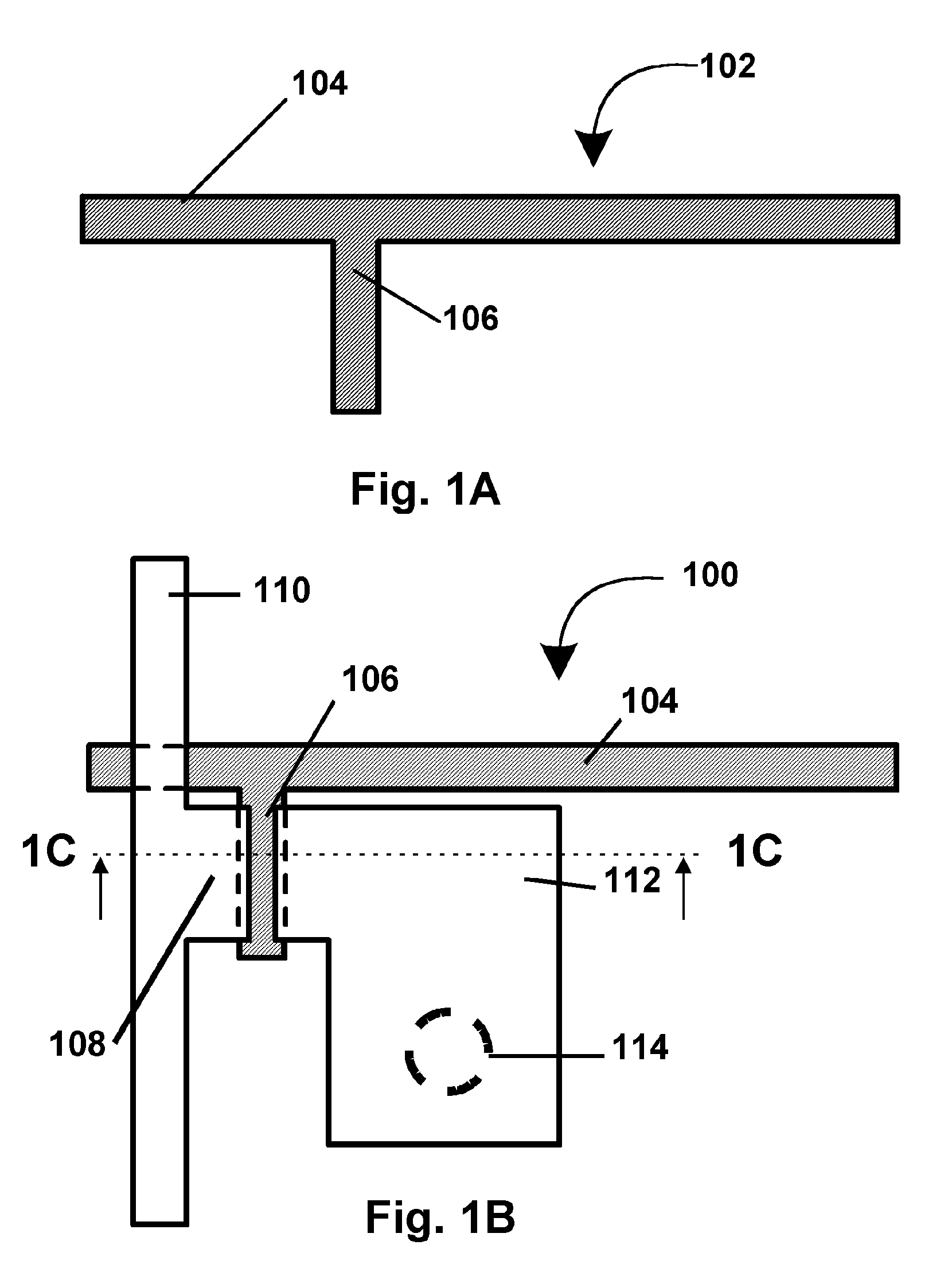
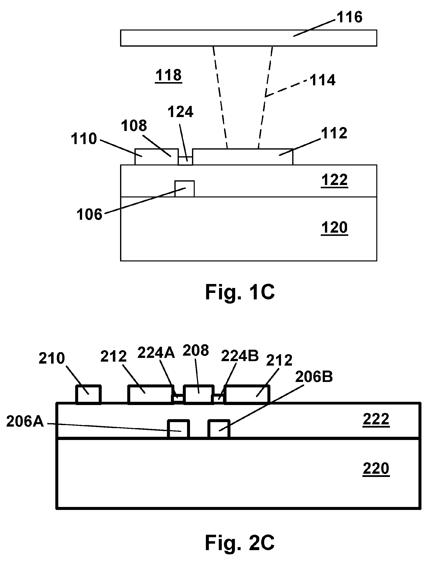
[0124]In the following detailed description, registration tolerant transistors will first be described with reference to FIGS. 1A-5. Next, processes for the formation of diodes and diode arrays by the processes of the present invention will be described with reference to FIG. 6A-8B. Screened source backplanes will then be described with reference to FIGS. 9A-10, and balance line backplanes will be described with reference to FIGS. 11-15. Finally, drivers of the present invention for driving balance line backplanes will be described with reference to FIGS. 16-20.

[0125]Registration-Tolerant Transistors

[0126]As already mentioned this invention provides a registration-tolerant transistor in which the gate electrode has two spaced edges and the drain electrode has first and second electrode edge portions which overlap the two spaced edges of the gate electrode to define two separate overlap areas, such that translation of the gate electrode relative to drain electrode (for example, due t...


PUM

PropertyMeasurementUnit
TFTaaaaaaaaaa
aspect ratioaaaaaaaaaa
contrastaaaaaaaaaa

Abstract

A thin-film transistor includes a gate electrode having first and second gate electrode edges on opposed sides, and a drain electrode having a first edge that overlaps the first gate electrode edge, and a second edge that overlaps the second gate electrode edge. A diode array is fabricated by successive deposition of a conductive layer, a doped semiconductor layer and an undoped semiconductor layer adjacent to the substrate. A display pixel unit provides reduced capacitative coupling between a pixel electrode and a source line. The source line includes an extension that provides a source for the transistor. A patterned conductive portion is disposed adjacent to the source line. Another display pixel unit provides reduced pixel electrode voltage shifts using a source line and a balance line.

Description

CROSS REFERENCE TO RELATED APPLICATIONS[0001]This application is a divisional of application Ser. No. 10 / 249,618, filed Apr. 24, 2003 (Publication No. 2003 / 0222315, now U.S. Pat. No. 7,116,318), which claims priority from Application Ser. Nos. 60 / 375,508 and 60 / 375,571, both filed Apr. 24, 2002.[0002]This application is also related to application Ser. No. 09 / 565,413, filed May 5, 2000 (now U.S. Pat. No. 7,030,412); application Ser. No. 09 / 904,109, filed Jul. 12, 2001 (Publication No. 2002 / 0106847, now U.S. Pat. No. 6,683,333); application Ser. No. 09 / 904,435, filed Jul. 12, 2001 (Publication No. 2002 / 0060321, now abandoned), and application Ser. No. 10 / 065,795, filed Nov. 20, 2002 (Publication No. 2003 / 0137521, now U.S. Pat. No. 7,012,600). This application is also related to application Ser. No. 10 / 249,624, filed Apr. 24, 2003 (Publication No. 2004 / 0014265, now U.S. Pat. No. 7,223,672). The entire contents of the aforementioned applications are herein incorporated by reference. Th...

Claims


Application Information

Patent Timeline
Patent Type & Authority Patents(United States)
IPC IPC(8): G09G3/34G02F1/163G02F1/15G02F1/167G09F9/30G09G3/20G09G3/38H01L21/336H01L21/77H01L21/84H01L27/12H01L29/417H01L29/423H01L29/786
CPCG09G3/344H01L27/1292H01L27/12H01L29/41733H01L29/42384H01L27/124H01L27/1285G09G3/2011G09G2300/043G09G2310/0262G09G2310/027G09G2310/0297G09G2320/0209H01L27/1214H01L27/1255
Inventor AMUNDSON, KARL R.CHEN, YUDENIS, KEVIN L.DRZAIC, PAUL S.KAZLAS, PETER T.RITENOUR, ANDREW P.
Owner E INK CORPORATION
Why Eureka
Try Eureka