Supercharge Your Innovation With Domain-Expert AI Agents!

Liquid crystal display panel capable of minimizing a defect rate caused by bright point and repairing method thereof

a liquid crystal display panel and defect rate technology, applied in non-linear optics, instruments, optics, etc., can solve the problems of wasting liquid crystal display panels with bright point defects, and affecting the marketability of the produ

Active Publication Date: 2009-11-03
LG DISPLAY CO LTD
View PDF17 Cites 4 Cited by
  • Summary
  • Abstract
  • Description
  • Claims
  • Application Information

AI Technical Summary

Benefits of technology

The patent text describes a liquid crystal display panel with a hole filled with an opaque substance located in the area corresponding to a bright point. The technical effect of this invention is to improve the display quality of the liquid crystal display panel by reducing the reflection of light from the bright point.

Problems solved by technology

However, if a particle is soundly settled between the thin films of both the upper array substrate 2 and the lower array substrate 32, the repair may be difficult with the rework or laser.
Accordingly, a problem that the particle is intermixed is frequently generated.
A liquid crystal display panel having a bright point defect may be wasted or subject to a substantially reduced marketability.

Method used


Image

  • Liquid crystal display panel capable of minimizing a defect rate caused by bright point and repairing method thereof
  • Liquid crystal display panel capable of minimizing a defect rate caused by bright point and repairing method thereof
  • Liquid crystal display panel capable of minimizing a defect rate caused by bright point and repairing method thereof

Examples


first embodiment

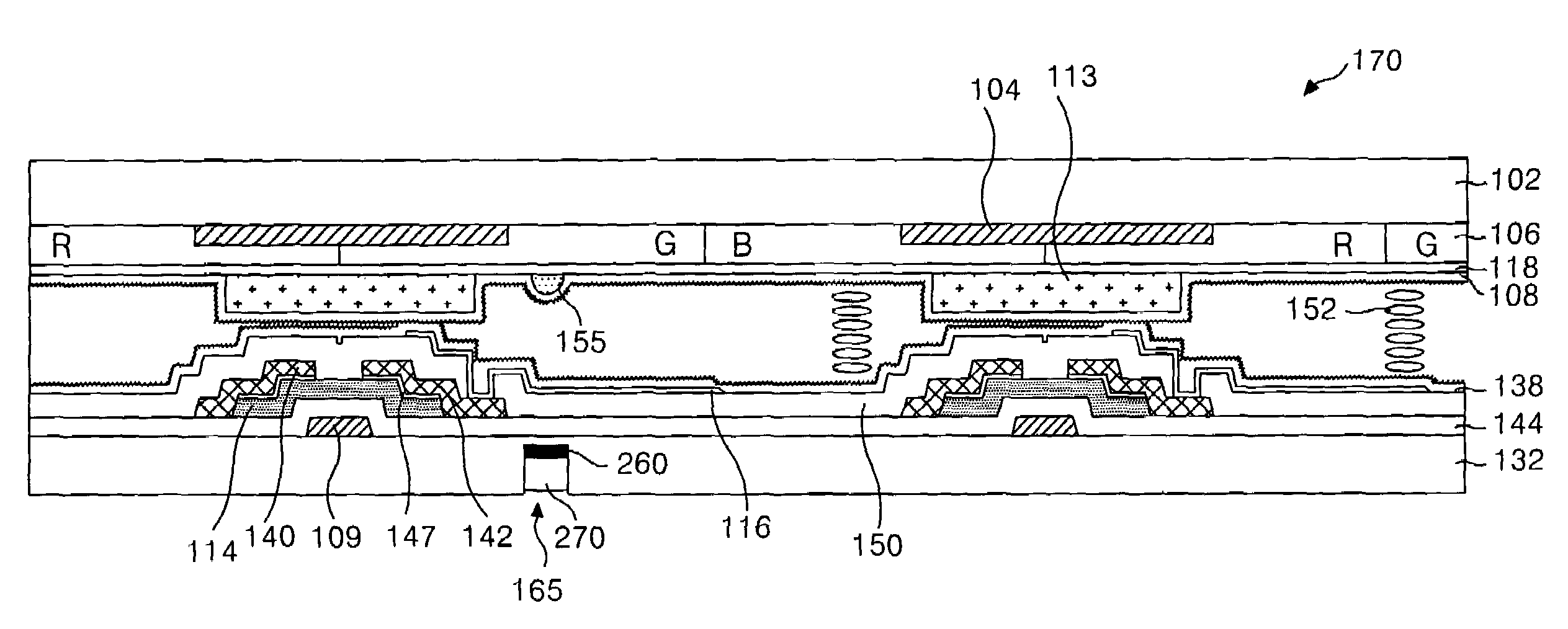
[0036]In FIGS. 6A-6E, a method of repairing the liquid crystal display panel of FIG. 4A is described. In FIGS. 6A-6E, the micro hole 165 is formed in the lower substrate 132. Accordingly, the lower substrate 132 is disposed in an upper position with respect to the upper substrate 102 for convenience of explanation in FIGS. 6A-6E. In other embodiment, the micro hole 165 may be formed in the upper substrate 102 or both the upper and lower substrates 102 and 132 upon needs.

[0037]In FIG. 6A, a bright point is generated in the liquid crystal display panel 170 by the particle 155 intermixed between the common electrode 118 and the upper alignment film 108. Accordingly, the micro hole 165 is formed in the lower substrate 132 corresponding to the area where the bright point is generated.

[0038]In this embodiment, the micro hole 165 is formed by using a micro drill. The micro hole 165 may be formed in a range of 20 μm to 500 μm in accordance with a size of the liquid crystal display panel 17...

second embodiment

[0043]FIGS. 7A to 7D illustrate a method of repairing the liquid crystal display panel 170 of FIG. 4A according to a In FIGS. 7A to 7D, the lower substrate 132 is shown at the upper position with respect to the upper substrate 102 for convenience of description only. In FIG. 7A, the colored pigment 410 such as a black or a gray pigment is dropped in the micro hole 165.

[0044]In FIG. 7B, the colored pigment 410 fully fills in the micro hole 165 to the extent that it slightly covers a surface of the lower array substrate 132. In FIG. 7C, an etchant is applied to remove the colored pigment 410 from an upper part of the micro hole 165. As a result, the colored pigment 410 remains only in some part of the micro hole 165, which is shown as a lower part of the micro hole 165 in FIG. 7D. After the colored pigment 410 is partially removed from the micro hole 165, the transparent pigment 420 may fill in the remaining part of the micro hole 165, as previously shown in FIGS. 6C and 6D.

third embodiment

[0045]FIGS. 8A to 8D illustrate a method of repairing the liquid crystal display panel 170 of FIG. 4A according to a In FIGS. 8A to 8D, the lower substrate 132 is illustrated at the upper position for convenience of description. In FIG. 8A, a colored electrode material 510 is deposited in the micro hole 165 on the lower substrate 132. The colored electrode material 510 is also deposited on the surface of the lower substrate 132, as shown in FIG. 8A. The colored electrode material 510 may include a black-colored electrode material such as chrome (Cr) or molybdenum (Mo) by using a deposition method.

[0046]In FIG. 8B, an etchant may be used to remove some of the colored electrode material 510 applied to the lower substrate 132. The colored electrode material 510 remains in some part of the micro hole 165 as a result of etching as shown in FIG. 8C. Because the micro hole 165 formed on the lower substrate 132 does not perfectly penetrate the lower substrate 132, the etchant may not reach...


PUM

PropertyMeasurementUnit
diameteraaaaaaaaaa
wavelengthaaaaaaaaaa
sizeaaaaaaaaaa

Abstract

A liquid crystal display penel includes a substrate, a hole disposed in the substrate, and an opaque substance filling in the hole. The hole is configured to be located in an area corresponding to a bright point. The liquid crystal display penel may minimize a defect ratio and improve a yield by darkening the bright point.

Description

[0001]This application claims the benefit of Korean Patent Applications Nos. P2005-50615 filed in Korea on Jun. 13, 2005, and P2005-71948 filed in Korea on Aug. 5, 2005, each of which is hereby incorporated by reference by its entirety.BACKGROUND[0002]1. Technical Field[0003]The invention relates to a liquid crystal display panel and repairing method thereof, and more particularly, to a repairing system of a liquid crystal display panel capable of minimizing a defect ratio and improving a yield.[0004]2. Related Art[0005]A liquid crystal display (LCD) device controls the light transmittance of a liquid crystal material in accordance with a video signal to display a picture. The liquid crystal display device includes a liquid crystal display panel in which liquid crystal cells are arranged in a matrix shape, and a drive circuit that drives the liquid crystal display panel.[0006]The liquid crystal display device is divided into two types in accordance with the electric field direction ...

Claims


Application Information

Patent Timeline
Patent Type & Authority Patents(United States)
IPC IPC(8): G02F1/1333G02F1/13
CPCG02F1/1309G02F1/136259
Inventor KWON, OH NAMNAM, SEUNG HEE
Owner LG DISPLAY CO LTD
Features
  • R&D
  • Intellectual Property
  • Life Sciences
  • Materials
  • Tech Scout
  • Unparalleled Data Quality
  • Higher Quality Content
  • 60% Fewer Hallucinations
Learn More