Solid state imaging device

a solid-state imaging and imaging device technology, applied in the direction of radioation control devices, instruments, television systems, etc., can solve the problems of ineffective directness of incident light to the light receiving elements, drawbacks of prior art light guides, etc., to reduce noise and small width

Inactive Publication Date: 2009-11-10
FUJIFILM CORP
View PDF4 Cites 10 Cited by
  • Summary
  • Abstract
  • Description
  • Claims
  • Application Information

AI Technical Summary

Benefits of technology

[0006]In view of the foregoing, an object of the present invention is to provide a solid state imaging device with light guides which direct light to light receiving elements efficiently.
[0012]According to the present invention, the light introduction region allows light from a wide area to enter the light guide, and directs the light to the light receiving element efficiently. Additionally, the reduced region that has a smaller width than the light introduction region prevents the light from entering the charge transfer paths around the light receiving element, and reduces the occurrence of noises.

Problems solved by technology

When the tapered shape is incorporated, however, some drawbacks arise in the prior art light guides.
In other words, with the tapered shape, the prior art light guides would not direct the incident light to the light receiving elements efficiently.

Method used


Image

  • Solid state imaging device
  • Solid state imaging device
  • Solid state imaging device

Examples


Embodiment Construction

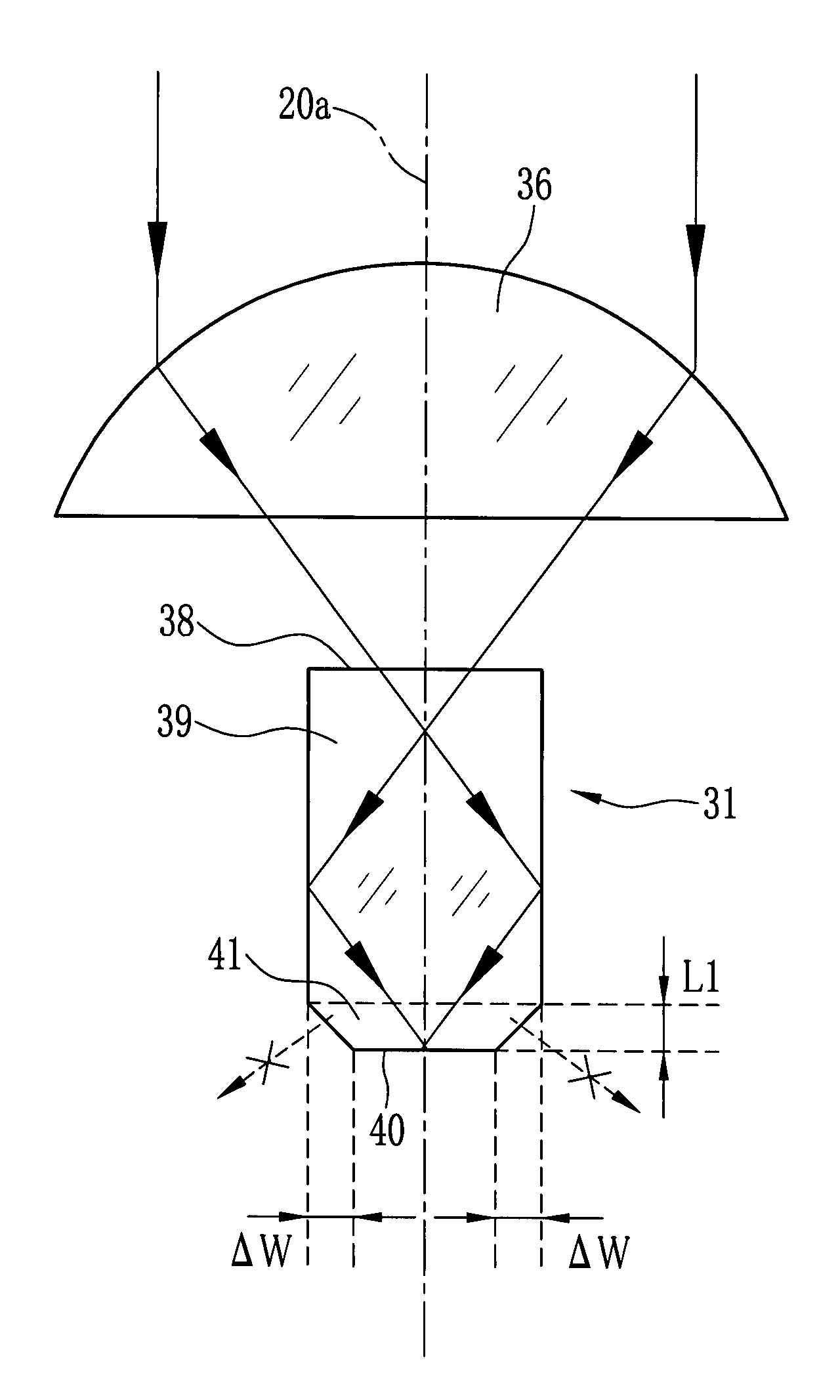
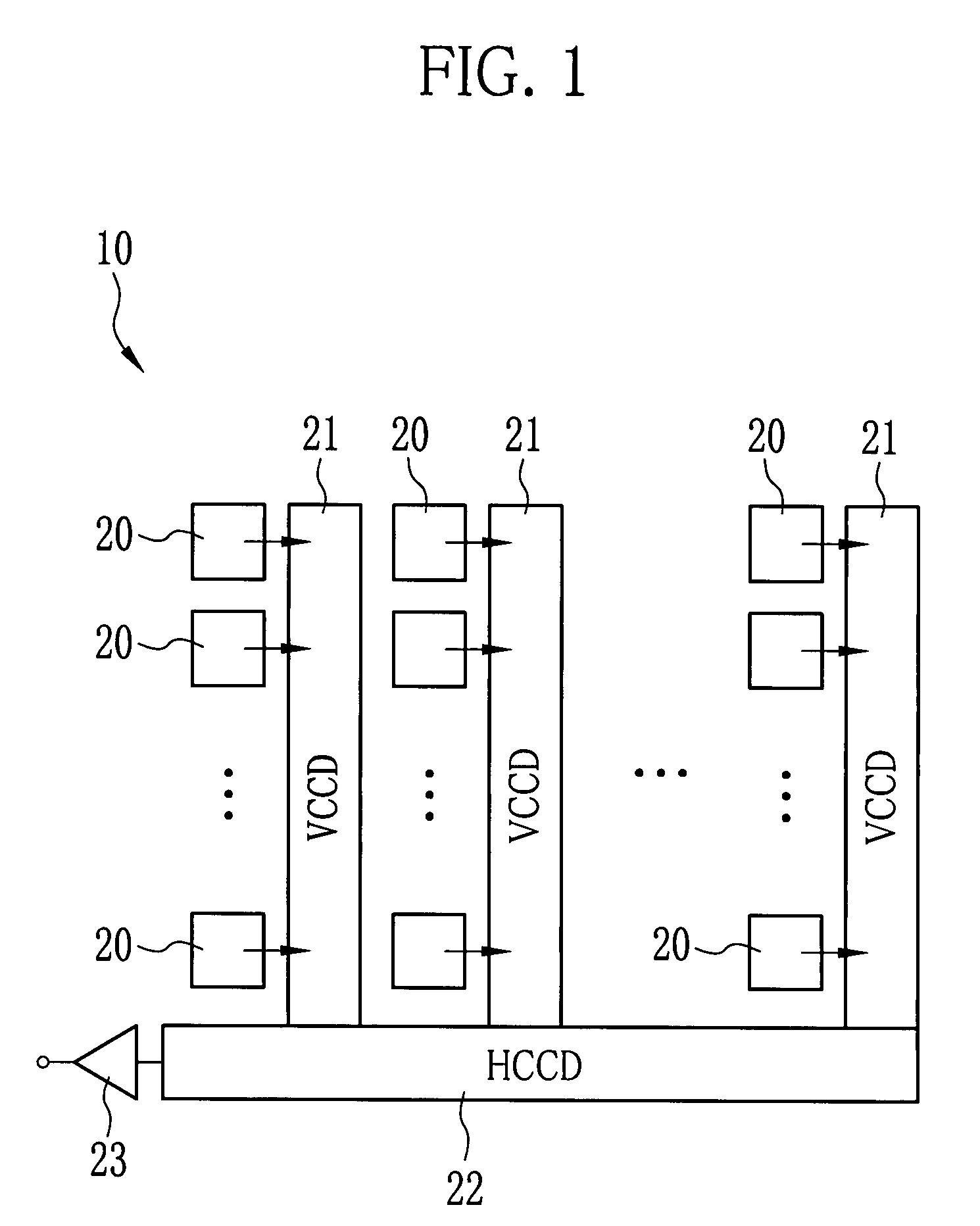
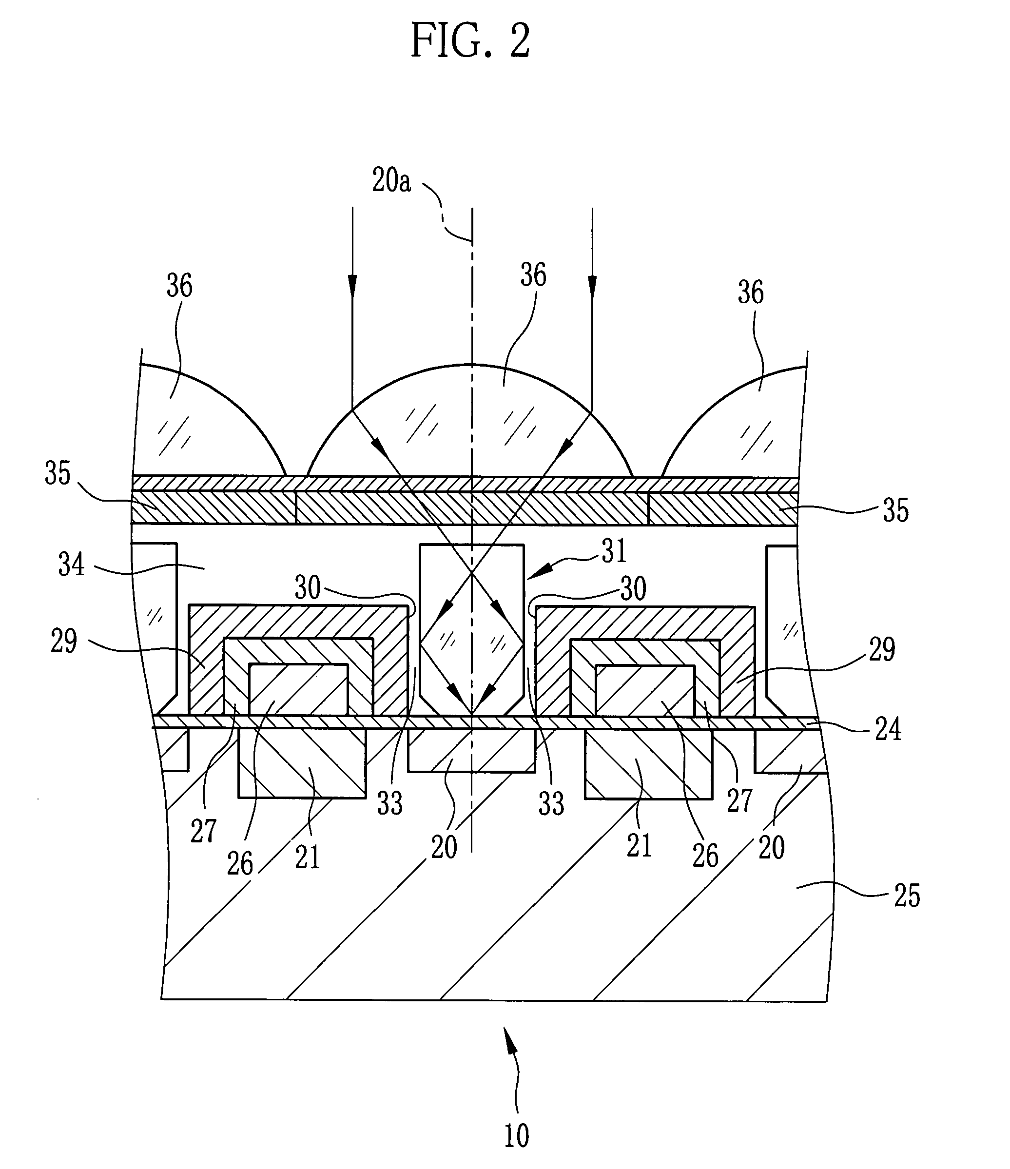
[0019]Referring to FIG. 1, a CCD image sensor 10 has a plurality of light receiving elements (photodiodes) 20 arranged in a two dimensional matrix form. The light receiving elements 20 convert light into an electrical signal equivalent to an amount of the light, and store this signal charge. The CCD image sensor 10 also has vertical transfer CCDs (VCCDs) 21 and a horizontal transfer CCD (HCCD) 22 which, in combination, transfer the signal charges of the light receiving elements 20 using an interline transfer method. The vertical transfer CCDs 21 extend along each column of the light receiving elements 20. The horizontal transfer CCD 22 is connected to the terminal ends of all the vertical transfer CCDs 21.

[0020]The signal charge in every light receiving element 20 is read out, all at once, into the vertical transfer CCDs 21 through transfer gates (not shown) in a predetermined readout cycle. The vertical transfer CCDs 21 transfer these signal charges, a step at a time, to the horizo...


PUM


Abstract

Light guides are formed above each light receiving element. These light guides are made of a high refractive index material, and surrounded by a material of lower refractive index. The light guides are each made up of a light introduction region leading with a constant width from a light entrance surface, and a tapered reduced region leading from the light introduction region to a light exit surface. The light introduction region totally reflects the incident light toward the reduced region. The reduced region, owing to its tapered shape, surely directs the light onto a light receiving element, and prevents the light from entering charge transfer paths around the light receiving element.

Description

FIELD OF THE INVENTION[0001]The present invention relates to a solid state imaging device with light guides to direct light onto light receiving elements.BACKGROUND OF THE INVENTION[0002]Solid state imaging devices, such as charge coupled device (CCD) image sensors and complementary metal oxide semiconductor (CMOS) image sensors, have been used as a solid state imaging device in digital cameras. Usually containing millions of light receiving elements (for example, photodiodes) which correspond to each pixel of a single chip and convert light into a signal charge, the solid state imaging devices output an image signal representative of an optical image formed by a lens system. To capture high definition images, the solid state imaging devices are becoming to have more pixels in these days. When more pixels are incorporated in the digital camera, each light receiving element necessarily becomes smaller, and the sensitivity of the digital camera decreases. Therefore, micro-lenses are c...

Claims


Application Information

Patent Timeline
Patent Type & Authority Patents(United States)
IPC IPC(8): H04N5/225G02B6/42H01L27/14H04N5/335H04N5/369H04N5/372H04N5/374
CPCH01L27/14625H01L27/14627H01L27/14806
Inventor TANI, TAKEHARU
Owner FUJIFILM CORP
Why Eureka
Try Eureka