Serial interface circuit for data transfer

a data transfer and serial interface technology, applied in the field of serial interface circuits, can solve the problems of increasing the consumption current of a large-scale integrated (lsi) circuit in standby, too high level to ignore, and off-transistor, so as to reduce the overhead of a cpu

Inactive Publication Date: 2009-11-10
LAPIS SEMICON CO LTD
View PDF2 Cites 0 Cited by
  • Summary
  • Abstract
  • Description
  • Claims
  • Application Information

AI Technical Summary

Benefits of technology

[0023]It is an object of the present invention to provide a serial interface circuit which can reduce a CPU overhead when a CPU accesses a peripheral circuit.
[0025]According to the present invention, the mirror register is connected to the CPU through a system bus, and holds the same data as the corresponding peripheral register. Therefore, the CPU can read and write data held in the peripheral register by performing parallel access to the mirror register through the system bus. This leads to a reduction of a CPU overhead when the CPU accesses the peripheral register.

Problems solved by technology

The use of the finer semiconductor process leads to an increase of the transistor off-leak current, thereby increasing the consumption current of a large-scale integrated (LSI) circuit in a standby state, where clock and input / output operations stop, to a too high level to ignore.
The reduction of the consumption current is a big issue especially for a portable device taking power from a battery.
As the number of the signal lines increases, an area occupied by the protection devices provided on the individual signal lines has become too large to ignore.

Method used


Image

  • Serial interface circuit for data transfer
  • Serial interface circuit for data transfer
  • Serial interface circuit for data transfer

Examples


first embodiment

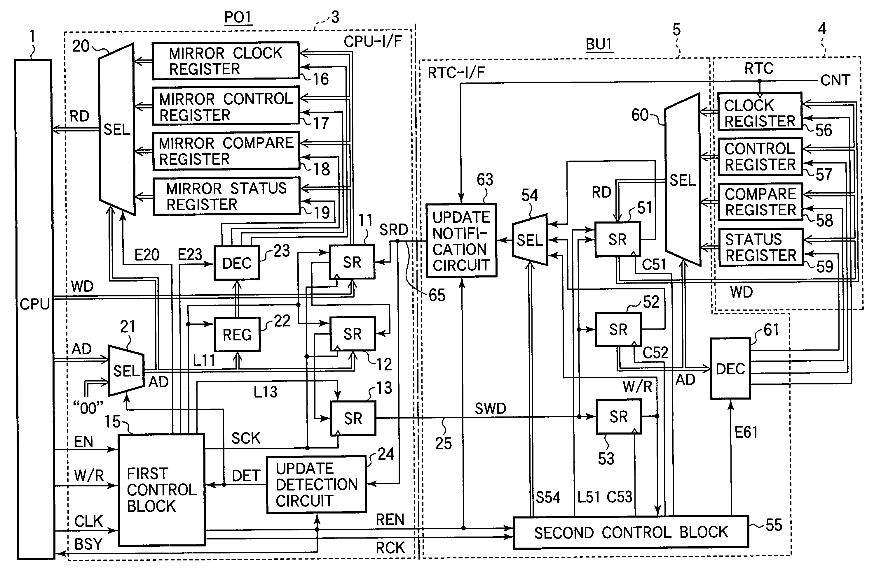
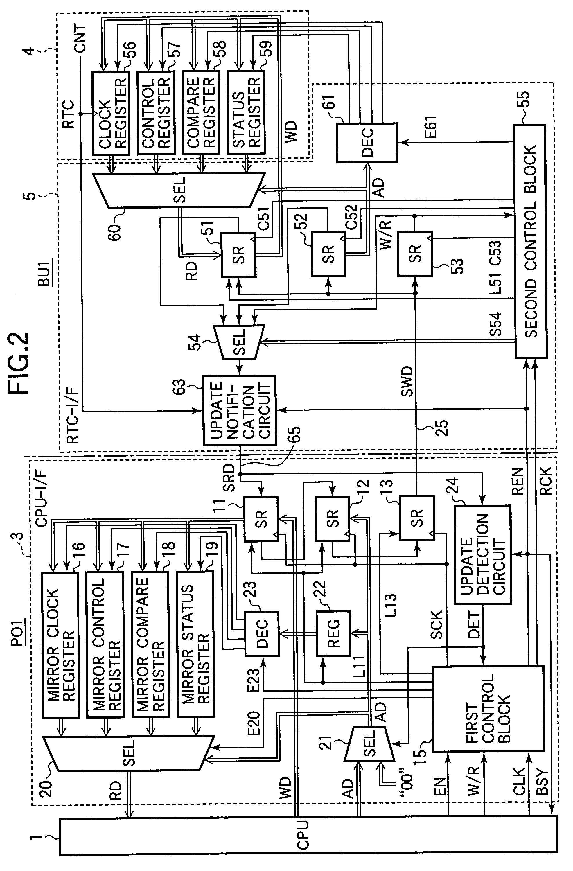
[0036]FIG. 2 is a diagram showing a configuration of a part of an LSI circuit including a serial interface circuit according to the first embodiment of the present invention. The parts in FIG. 2 that are identical to or correspond to the parts in FIG. 1 are assigned identical reference characters.

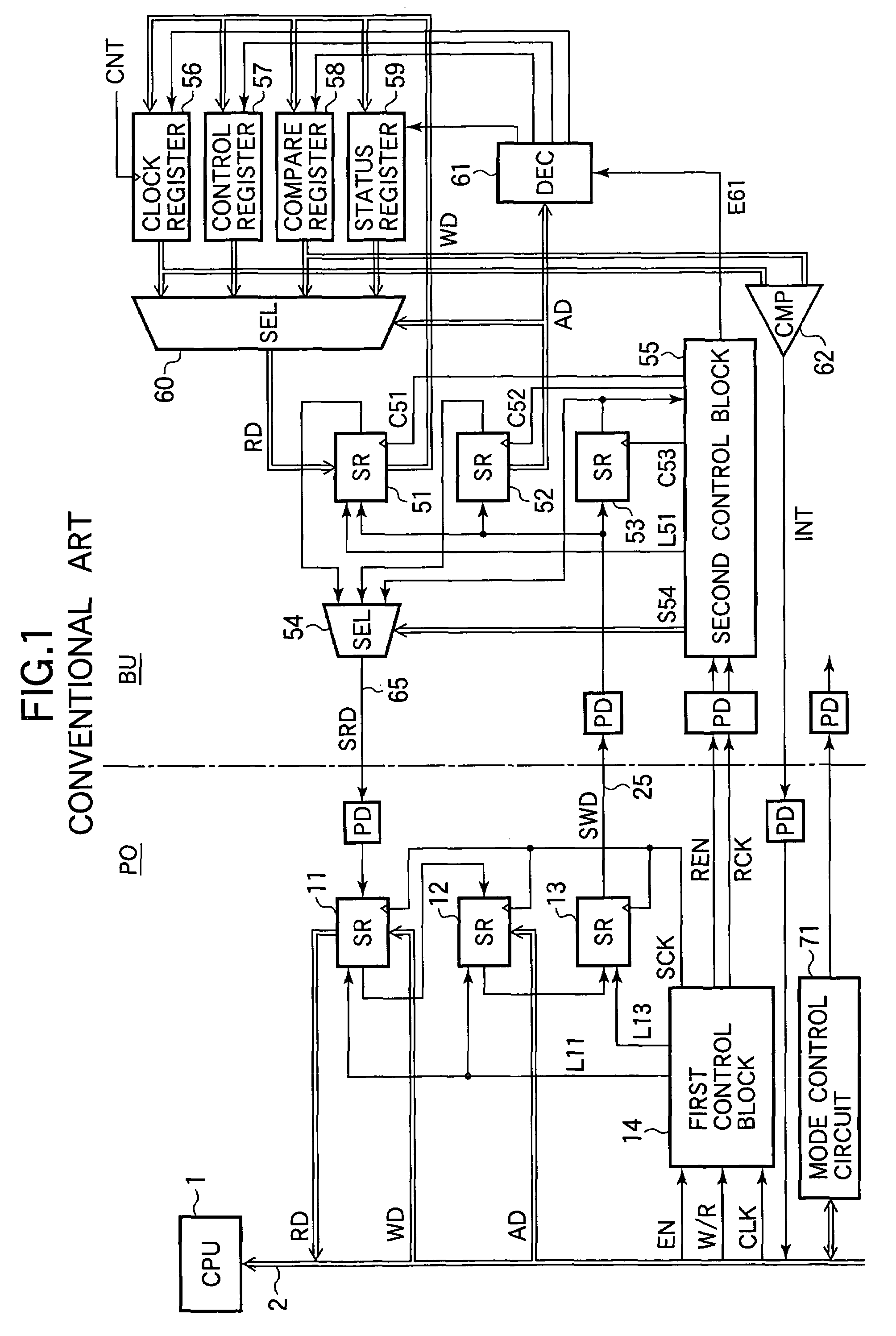
[0037]Referring to FIG. 2, the LSI circuit includes a power-off area portion PO1 as a core portion of the LSI circuit and a backup area portion BU1 as a peripheral circuit of the LSI circuit. As shown in the left half of FIG. 1, the power-off area portion PO1 includes a CPU 1 and a CPU interface (CPU-I / F) 3. As shown in the right half of FIG. 1, the backup area portion BU1 includes a real time clock (RTC) portion 4 including an internal clock (not shown), and a real time clock interface (RTC-I / F) 5. Power is not supplied to the power-off area portion PO1 as the core portion of the LSI circuit in a standby state. On the other hand, power is supplied to the backup area portion BU1 as the peri...

second embodiment

[0088]FIG. 5 is a diagram showing a configuration of a part of an LSI circuit including a serial interface circuit according to the second embodiment of the present invention. The parts in FIG. 5 that are identical to or correspond to the parts in FIG. 2 are assigned the identical reference characters.

[0089]Referring to FIG. 5, the serial interface circuit according to the second embodiment includes a mirror clock register 16A which increments in accordance with a count signal CNT in the same way as the clock register 56 in the backup area portion BU2, instead of the mirror clock register 16 in the power-off area portion PO1 shown in FIG. 2. The serial interface circuit according to the second embodiment also includes a logic gate 24A instead of the update detection circuit 24 in the power-off area portion PO1 shown in FIG. 2. The logic gate 24A outputs an update detection signal DET when an interrupt signal INT is sent from the backup area portion BU2 while an operation enable sign...

third embodiment

[0095]FIG. 6 is a diagram showing a configuration of a part of a serial interface circuit according to the third embodiment of the present invention. The parts in FIG. 6 that are identical to or correspond to the parts in FIG. 5 are assigned the identical reference characters. In FIG. 6, just the power-off area portion PO3 of the serial interface circuit according to the third embodiment is shown. The backup area portion BU3 of the serial interface circuit according to the third embodiment is the same as that according to the second embodiment shown in FIG. 5.

[0096]Referring to FIG. 6, the serial interface circuit according to the third embodiment includes a mirror status register 19A instead of the mirror status register 19 shown in FIG. 5, and data held in the mirror status register 19A can be set by an interrupt signal INT. The other elements in FIG. 6 are the same as those in FIG. 5.

[0097]If the interrupt signal INT is generated in the backup area portion BU3 of the serial inter...


PUM


Abstract

A serial interface circuit includes a first circuit disposed in the core portion and connected to the CPU, and a second circuit disposed in the peripheral circuit and connected to the peripheral registers and the first circuit; the first circuit including mirror registers, shift registers, in the write operation, serially outputting write data to the second circuit, and in the read operation, serially receiving read data supplied from the second circuit, and a first control block, in the read operation, generating a timing signal for writing the read data held in the shift registers into the corresponding mirror registers; the second circuit including shift registers and a second control block generating a second timing signal for either writing the write data held in the second shift register into the corresponding peripheral register or outputting data held in the peripheral register to the second shift register.

Description

BACKGROUND OF THE INVENTION[0001]1. Field of the Invention[0002]The present invention relates to a serial interface circuit for use when a central processing unit (CPU) accesses a peripheral circuit, and more particularly, to a reduction of the CPU overhead when a CPU accesses a peripheral circuit.[0003]2. Description of the Related Art[0004]The use of the finer semiconductor process leads to an increase of the transistor off-leak current, thereby increasing the consumption current of a large-scale integrated (LSI) circuit in a standby state, where clock and input / output operations stop, to a too high level to ignore. The reduction of the consumption current is a big issue especially for a portable device taking power from a battery. One of the most effective methods for reducing the consumption current in a standby state is to shut off power to the LSI circuit.[0005]In a case of an LSI circuit which shuts off the entire circuit when powering off, there is no problem to use a usual ...

Claims


Application Information

Patent Timeline
Patent Type & Authority Patents(United States)
IPC IPC(8): G06F3/00G06F1/04G06F1/12G06F13/12
CPCG06F13/385
Inventor HIRASAWA, MASAYUKIWATANABE, MITSUHIRO
Owner LAPIS SEMICON CO LTD
Why Eureka
Try Eureka