Optical inspection using variable apodization

Active Publication Date: 2009-11-17
APPL MATERIALS ISRAEL LTD
View PDF16 Cites 14 Cited by
  • Summary
  • Abstract
  • Description
  • Claims
  • Application Information

AI Technical Summary

Benefits of technology

[0008]Proper selection of the characteristics of the aperture and the spatial filter permits the SNR of the detector to be optimized for each type of substrate pattern that the inspection system encounters. This optimization involves choosing the size and shape of the aperture so as to reduce the background level, typically by narrowing the

Problems solved by technology

There are many cases, however, in which the interference lobes occupy substantially the entire field of view of the detector, so that blocking the lobes is impossible without entirely blocking the detector.
Ev

Method used


Image

  • Optical inspection using variable apodization
  • Optical inspection using variable apodization
  • Optical inspection using variable apodization

Examples


Example

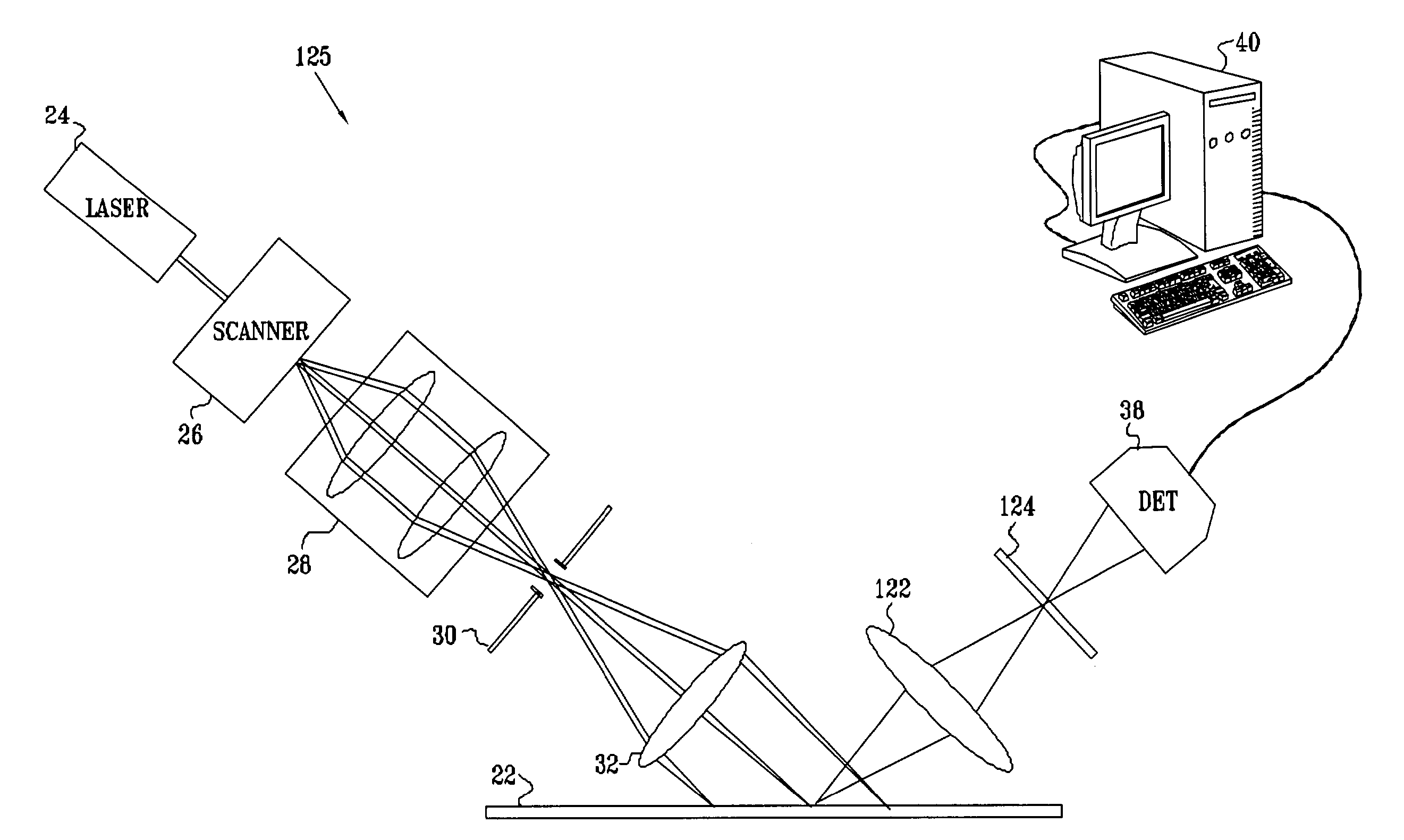
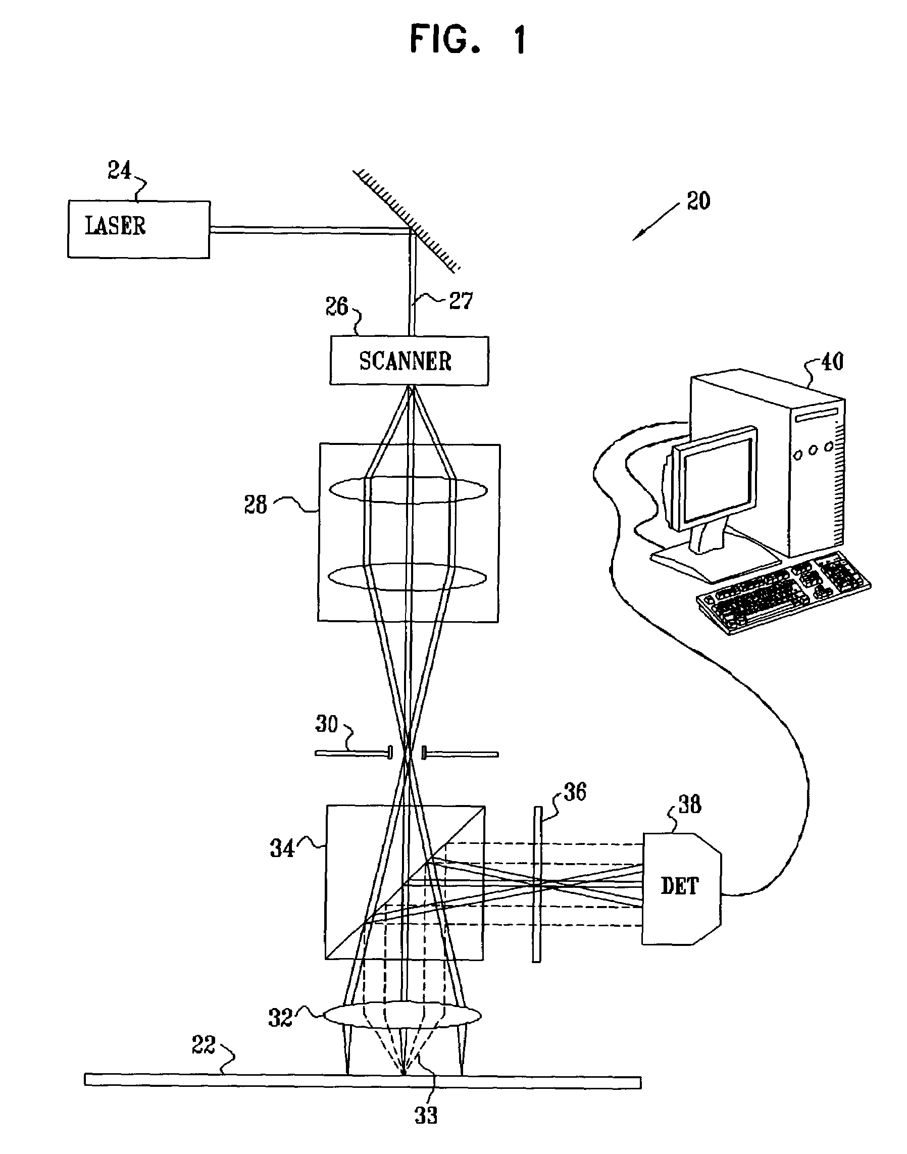
[0067]FIG. 1 is a schematic side view of a system 20 for optical inspection of a substrate 22, in accordance with an embodiment of the present invention. System 20 is designed for detecting defects in integrated circuit (IC) wafers, and applies apodization techniques, as described hereinbelow, that are particularly useful in suppressing background scattering due to patterns formed on the wafer surface. Patterns of this sort are encountered in many types of ICs, but particularly in memory devices, such as SRAM and DRAM chips. Therefore, in the description that follows of system 20 and of various apodization schemes that can be used in the system, reference is made to such patterns. It should be understood, however, that these references to IC patterns are made by way of example, and the principles of the present invention may similarly be applied to inspection of surfaces of other types. In particular, the principles of system 20 may be applied, mutatis mutandis, to inspection of lit...


PUM


Abstract

A method for optical inspection of a surface includes selecting an apodization scheme in response to a characteristic of the surface, and applying an apodizer to apodize a beam of radiation in response to the selected apodization scheme. The apodized beam of radiation is directed to impinge on the surface, whereby a plurality of rays are scattered from the surface, and at least one of the scattered rays is detected, typically in order to detect a defect on the surface.

Description

CROSS-REFERENCE TO RELATED APPLICATION[0001]This application claims the benefit of U.S. Provisional Patent Application No. 60 / 349,662, filed Jan. 15, 2002, which is incorporated herein by reference.FIELD OF THE INVENTION[0002]The present invention relates generally to methods and systems for automated optical inspection, and specifically to methods for enhancing sensitivity of optical inspection systems that are used for defect detection.BACKGROUND OF THE INVENTION[0003]Laser scanning systems are well known in the art of optical inspection. Typically, a laser beam scans over the substrate under inspection, and the light scattered from the substrate is collected by a detector. The intensity (and possibly other characteristics) of the scattered light is compared to an expected range of values. Deviations of the scattered light from the expected range can be indicative of defects in or on the substrate. In integrated circuit (IC) manufacturing, for example, as the laser beam scans the ...

Claims


Application Information

Patent Timeline
IPC IPC(8): G01N21/00G01N21/88
CPCG01N21/8806
Inventor MILSHTEIN, EREL
Owner APPL MATERIALS ISRAEL LTD
Why Eureka
Try Eureka