Memory built-in self repair (MBISR) circuits/devices and method for repairing a memory comprising a memory built-in self repair (MBISR) structure

a self-repairing and memory technology, applied in error detection/correction, digital storage, instruments, etc., can solve the problems of discarded memories which might be recovered instead, excessive waste of spare cells, and inability to use memory, so as to optimize the allocation of available redundant resources, improve performance, and improve performan

Inactive Publication Date: 2009-12-01
INFINEON TECH AG
View PDF25 Cites 23 Cited by
  • Summary
  • Abstract
  • Description
  • Claims
  • Application Information

AI Technical Summary

Benefits of technology

[0017]It is an object of the present invention to provide a method for repairing a memory comprising a Memory Built-In Self Repair (MBISR) structure, which has an improved performance in comparison with the above described methods known from the state of the art, and to provide Memory Built-In Self Repair (MBISR) devices and Memory Built-In Self Repair (MBISR) circuits having an improved performance in comparison with Memory Built-In Self Repair (MBISR) devices and Memory Built-In Self Repair (MBISR) circuits from the state of the art, respectively. For some embodiments, a Memory Built-In Self Repair (MBISR) structure and a redundancy allocation method with related circuit infrastructure are utilized to combine classical repair strategies (row and column replacement) with new approaches (word replacement) to optimize the allocation of available redundant resources and to achieve the highest possible repair rate for any given memory configuration.
[0018]In this distributed Memory Built-In Self Repair (MBISR) structure, each memory array with row and column redundancies is provided with dedicated circuitry (Row / Column MBISR) which automatically allocates spare array resources to those rows and columns containing defects. In comparison with centralized Memory Built-In Self Repair (MBISR) structures known from the state of the art such a distributed Memory Built-In Self Repair (MBISR) structure according to embodiments of the present application has the advantage that it allows MBISR (Memory Built-In Self Repair) and MBIST (Memory Built-In Self Test) to be carried out simultaneously, thus saving testing time and money. The device and circuit structures according to embodiments of the present invention may allow fast calculation of spare row / column allocation without impacting the duration of MBIST (Memory Built-In Self Test) tests. Minimal hardware overhead is required for typical row / column redundancy implementations according to the invention. For some embodiments, memory arrays with MBISRs may be grouped to form larger memory subsystems. Either single or grouped arrays may be provided with a set of shared spare words which are used to repair faulty cells not covered by row and column redundancies.
[0019]When used in combination with word redundancies, the circuits allow minimizing the number of spare rows and columns, thus leading to significant reductions in system area, power, and cost. One single MBIST may serve multiple memories with row / column and word redundancies.
[0020]The method described herein may be used to optimize the usage of available spare memory resources. The technique utilizes a relatively simple algorithm which can be implemented with minimal hardware overhead in case of low spare row / column count. The technique is also scalable, as the number of faulty row / column registers depends on the number of spare rows and columns, not on the memory array size.

Problems solved by technology

Due to uncontrollable factors, memories may contain randomly distributed defective cells after fabrication which cause the memory to be unusable even if faults affect very small parts of the entire cell array.
Generally, complex processing is required to identify optimal repair configurations; in addition, optimal repair configurations may not even be identified due to inefficient processing, thus leading to discarded memories which might be recovered instead.
This simple criteria leads to excess waste of spare cells whenever the number of faulty cells in one row / column is significantly less than the total cells replaced.
Such word replacement is more flexible than row and column replacement in that it allows fixing sparse faulty cells, but it is not suitable for repairing column or periphery defects and, to some extent, row defects.
Optimal repair configurations may not be identified due to inefficient processing, thus leading to discard memories which might be repaired instead.

Method used


Image

  • Memory built-in self repair (MBISR) circuits/devices and method for repairing a memory comprising a memory built-in self repair (MBISR) structure
  • Memory built-in self repair (MBISR) circuits/devices and method for repairing a memory comprising a memory built-in self repair (MBISR) structure
  • Memory built-in self repair (MBISR) circuits/devices and method for repairing a memory comprising a memory built-in self repair (MBISR) structure

Examples


Embodiment Construction

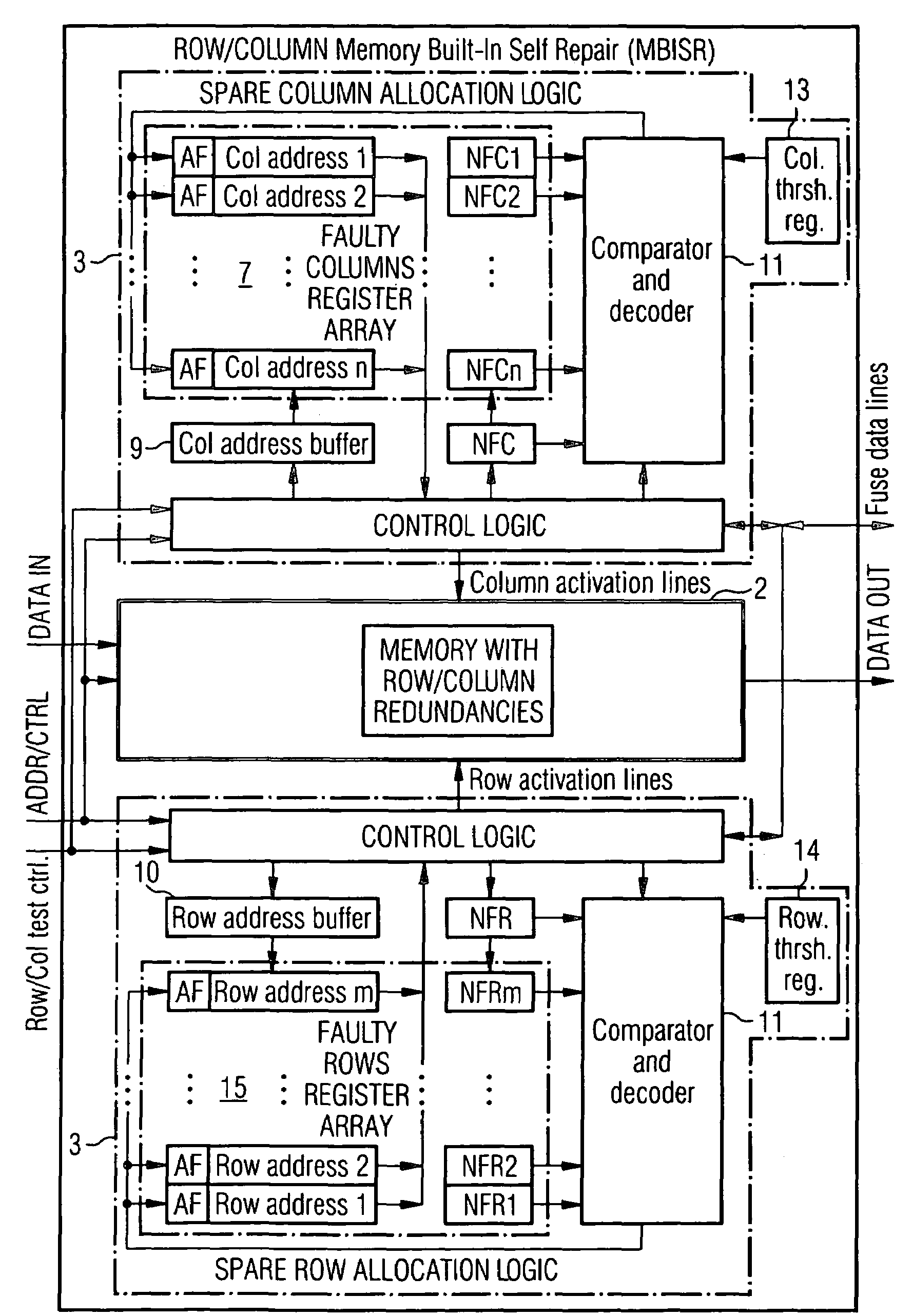
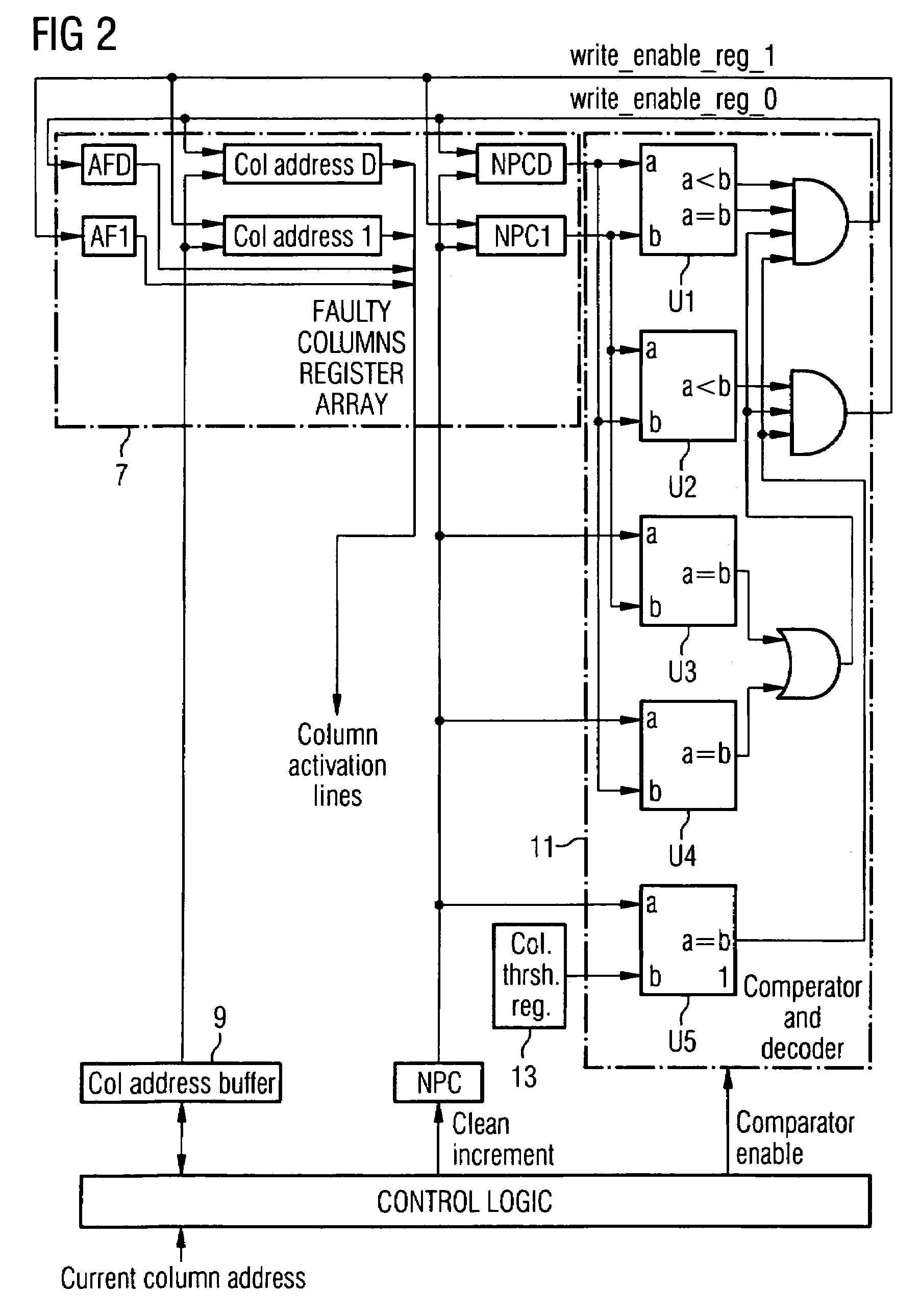
[0032]Circuit infrastructure needed to implement a spare row / column allocation as part of an embodiment of the method according to the invention is shown in FIGS. 1 and 2, wherein FIG. 2 is a more detailed representation of a Column Memory Built-In Self Repair (MBISR) circuit 3, which Column Memory Built-In Self Repair (MBISR) circuit 3 is part of the scheme of FIG. 1. Each memory array 2 (see also FIG. 3) with a given amount of spare rows and columns is provided with two independent spare row / column allocation circuits (Memory Built-In Self Repair (MBISR) circuits) 3, i.e. one Column Memory Built-In Self Repair (MBISR) circuit (see FIG. 2), and one Row Memory Built-In Self Repair (MBISR) circuit. It has to be understood that in the present example the principle structures of the Column Memory Built-In Self Repair (MBISR) circuit and of the Row Memory Built-In Self Repair (MBISR) circuit are the same. Hence, the detailed scheme of FIG. 2 showing an embodiment of the Column Memory Bu...


PUM


Abstract

A method for repairing a memory comprising a Memory Built-In Self Repair (MBISR) structure comprises the steps of detection of defective storage cells, and redundancy allocation. The redundancy allocation step is carried out in such a way that it combines a row and / or column oriented redundancy repair approach with a word oriented redundancy repair approach. A Memory Built-In Self Repair (MBISR) device comprises at least one memory (2) with row and / or column redundancy, at least one row and / or column Memory Built-In Self Repair (MBISR) circuit (3), and a word redundancy block (4). Furthermore, a distributed MBISR structure as well as dedicated Column / Row MBISR circuits (3) are provided.

Description

CROSS-REFERENCE TO RELATED APPLICATIONS[0001]This application claims foreign priority benefits under 35 U.S.C. §119 to co-pending European patent application number 03 002 698.3, filed Feb. 12, 2003. This related patent application is herein incorporated by reference in its entirety.BACKGROUND OF THE INVENTION[0002]1. Field of the Invention[0003]The invention relates to methods and devices for repairing a memory utilizing a Memory Built-In Self Repair (MBISR) structure.[0004]2. Description of the Related Art[0005]Digital memories typically consist of two-dimensional arrays of elements (storage cells) each capable of storing N different data values, where N is the number of stable states of the storage cell. The cells of the array are arranged into rows and columns.[0006]Due to uncontrollable factors, memories may contain randomly distributed defective cells after fabrication which cause the memory to be unusable even if faults affect very small parts of the entire cell array. The la...

Claims


Application Information

Patent Timeline
Patent Type & Authority Patents(United States)
IPC IPC(8): G11C29/00G11C7/00H02H3/05
CPCG11C29/81G11C29/72
Inventor DI RONZA, MARIOMARTELLONI, YANNICK
Owner INFINEON TECH AG
Why Eureka
Try Eureka