Structure, optical device, magnetic device, magnetic recording medium and manufacturing method thereof

a technology of optical devices and manufacturing methods, applied in the field of structures, optical devices, magnetic devices, magnetic recording mediums and manufacturing methods thereof, can solve the problems of reducing the degree of adsorption of magnetic materials, limiting the recording density, and being extremely difficult to form a high aspect structure which is realized by the anodization method

Inactive Publication Date: 2009-12-22
CANON KK
View PDF9 Cites 8 Cited by
  • Summary
  • Abstract
  • Description
  • Claims
  • Application Information

AI Technical Summary

Problems solved by technology

A longitudinal recording system, which is the current mainstream of magnetic recording media, becomes more liable to demagnetization as the recording density increases and limitation of its recording density is pointed out.
The above described nano structure is generally formed using a lithography technology and etching technology, but using such techniques, it is extremely difficult to form a high aspect structure which is realized by the anodization method.
Furthermore, the above described magnetic recording medium is disk-shaped and the rotator when information is recorded or reproduced is subject to fine vibration or eccentricity, which prevents recorded tracks from becoming concentric, producing position errors of the head and tracks.
Similar position errors are also produced by deformation due to expansion of the disk caused by a thermal distribution in the apparatus.
Therefore, the recording area is divided into data areas for recording information and servo areas for detecting track positions and positions are corrected while the head is detecting position information of tracks, but patterned media which are being developed in recent years have a problem as to how to construct servo areas.

Method used


Image

  • Structure, optical device, magnetic device, magnetic recording medium and manufacturing method thereof
  • Structure, optical device, magnetic device, magnetic recording medium and manufacturing method thereof
  • Structure, optical device, magnetic device, magnetic recording medium and manufacturing method thereof

Examples


embodiment 1

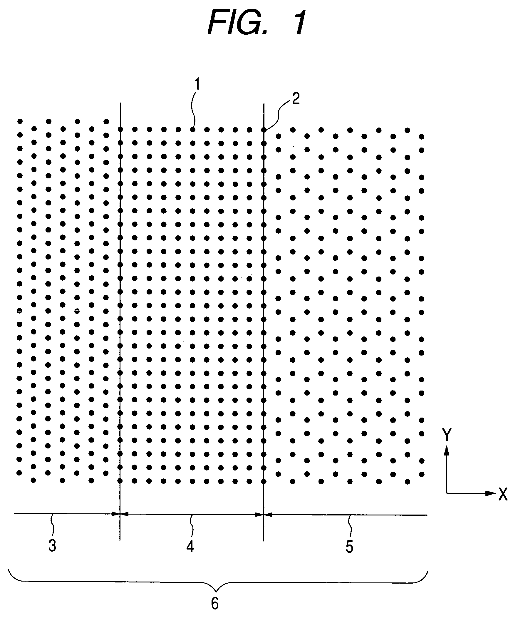
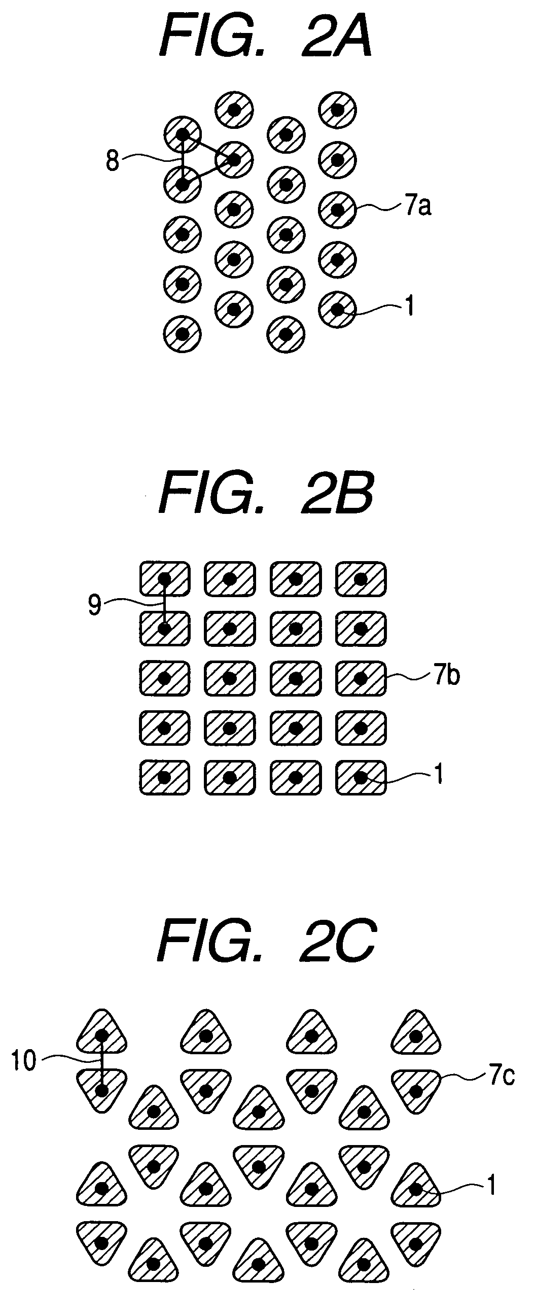
[0055]First, as step (2), concave structures having desired arrays are formed on the surface of a substrate on which an aluminum thin film is formed using an electron beam direct drawing method and these are used as pore starting points. As shown in FIG. 1, the array of pore starting points 1 consists of a hexagonal lattice area 3, a rectangular lattice area 4 and a graphite-shaped lattice area 5 affanged adjacent to one another and pores 2 on the boundary of the adjacent areas are shared by both areas. That is, the two adjacent areas share an away of pores with equal periodicity on the boundary. Black bullets 1 in FIGS. 2A to 2C indicate projected positions of pores on a plane of the hexagonal lattice area, rectangular lattice area and graphite-shaped lattice area in FIG. 1. In FIGS. 2A to 2C, a period 8 of the hexagonal lattice area 3 is 200 nm, a period 9 of the rectangular lattice area 4 in the Y direction is 200 nm, that of the X direction is 250 nm and the most proximate dista...

embodiment 2

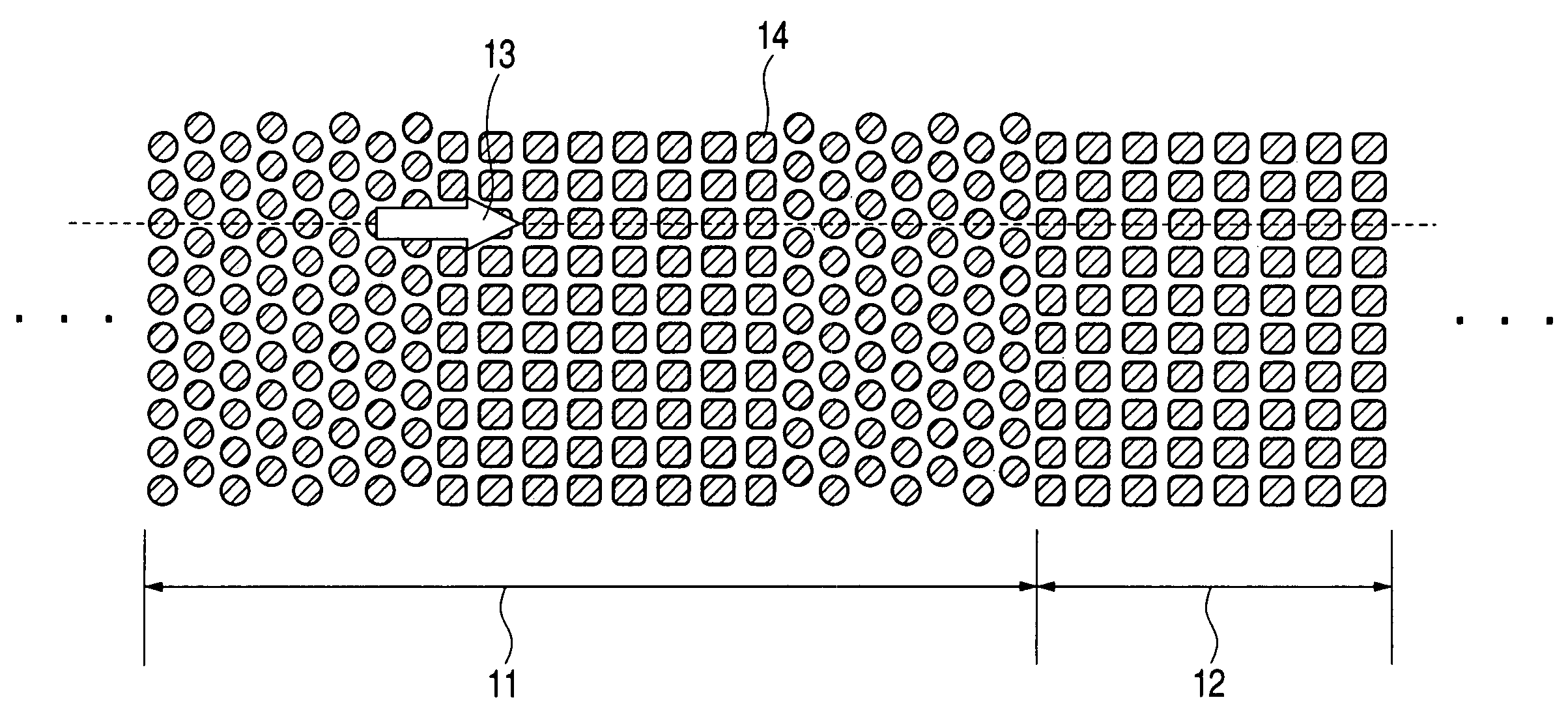
[0058]As a magnetic device, pores with hexagonal lattice areas and rectangular lattice areas having the same period as that of Embodiment 1 which are repeatedly arranged adjacent to one another are formed. FIG. 3 shows arrays of pores. The method of formion is the same as that in Embodiment 1. Cobalt is charged into the pores formed by an electric plating method to convert the area to a magnetic recording area. In this magnetic device, a direction 13 is regarded as the track orientation and the magnetic device is used, divided into a servo area 11 and data area 12. Some magnetic substance cell groups in the servo area are half a period shifted from the period of the magnetic substance cell groups in the direction perpendicular to the track direction and this is effective for performing position control (called “off track”) of the head and tracks. This prevents information of the adjacent tracks from being mistakenly reproduced or information from being overwritten on the already rec...

embodiment 3

[0059]As a device, pores with hexaganol lattice areas arranged on both sides of a rectangular lattice area formed. The method of formation is the same as that of Embodiment 1 and then polystyrene with light-emitting pigment is charged into the pores. Since the photonic band structure of the rectangular lattice area is different from that of the hexagonal lattice area, wavelengths which are easily guided vary depending on their respective structures. For this reason, when light wave which propagates through the rectangular lattice area but does not propagate through the hexagonal lattice area is introduced into the pores in the rectangular lattice area in the vertical direction 16 (see FIG. 4) and if this structure is regarded as a light waveguide, the rectangular lattice area becomes a core and the hexagonal lattice area becomes a cladding and light wave propagates with lower loss compared with a normal two-dimensional light waveguide. Filling arbitrary pores in the core area with a...


PUM

PropertyMeasurementUnit
distanceaaaaaaaaaa
sizeaaaaaaaaaa
lattice structureaaaaaaaaaa

Abstract

A nano structure having pore array structures in which a plurality of periodic arrays are formed adjacent to one another and a method of manufacturing the nano structure are provided. A nano structure having periodic array structures of pores formed in an anodized oxide film with a plurality of types of the periodic array structures arranged adjacent to one another is provided. Furthermore, a method of manufacturing a nano structure in which a plurality of periodic array structures formed in an anodized oxide film having different periods are arranged adjacent to one another, including (1) a step of forming pore starting points made up of a plurality of types of periodic arrays on the surface of a substrate comprised of aluminum as a principal component and (2) a step of anodizing the substrate simultaneously at the same anodization voltage is provided.

Description

TECHNICAL FIELD[0001]The present invention relates to a structure having concavo-convex structures on the order of nanometers arranged at intervals on the scale of nanometers (hereinafter also referred to as a “nano structure”), an optical device, a magnetic device, a magnetic recording medium, and a method of manufacturing the structure.BACKGROUND ART[0002]As a technology of forming a nanostructure or microstructures on the surface of an object, a technology of forming pores of several hundred nm or less in size using an anodization for a film or substrate comprised of aluminum as a principal component rather than a lithography technology using light rays or electron beams is conventionally known.[0003]The anodization method is a method applying an electric field to a substrate comprised of aluminum as a principal component as an anode in an acid bath oxidation and a dissolution phenomenon and form pores on the surface of the substrate. These pores are formed straightforward in the...

Claims


Application Information

Patent Timeline
Patent Type & Authority Patents(United States)
IPC IPC(8): G11B5/09G02B6/12B82B1/00C25D11/04C25D11/18G11B5/65G11B5/73G11B5/84G11B5/855H01L29/06
CPCB82Y10/00B82Y20/00C25D11/045G11B5/743G11B5/855G02B6/1225
Inventor IMADA, AYADEN, TOHRU
Owner CANON KK
Why Eureka
Try Eureka