

Synchronous memory having shared CRC and strobe pin
- Summary
- Abstract
- Description
- Claims
- Application Information
AI Technical Summary
Benefits of technology
Problems solved by technology
Method used
Image

Examples
Embodiment Construction
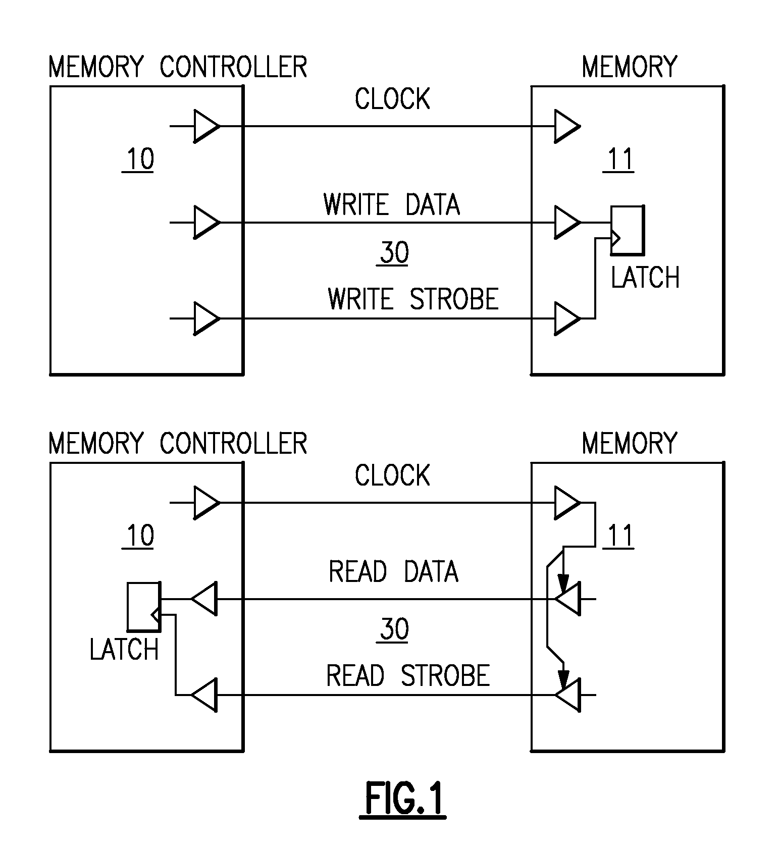
[0017]Turning now to the drawings in greater detail, it will be seen that in FIG. 1 there is illustrated a memory controller 10 and a memory storage device (DRAM or DIMM of DRAMs) 11 which have a data communication bus 30 there between. The illustrated coupling of FIG. 1 has no CRC pins but has strobe pins. The memory controller and the DRAM have latches which are used for the timed signals (which are timed by the Clock signal) being transmitted from one element to the other, from the driver in the Memory controller to the receiver in the memory chip. In the case of a strobe, the strobe signal becomes a timed input to the memory chip's latch for data, be it read or write. In each of the illustrated diagrams, the memory controller and DRAM each have three pins. In FIG. 1 there are as illustrated, pins for Clock, Data, and Strobe.
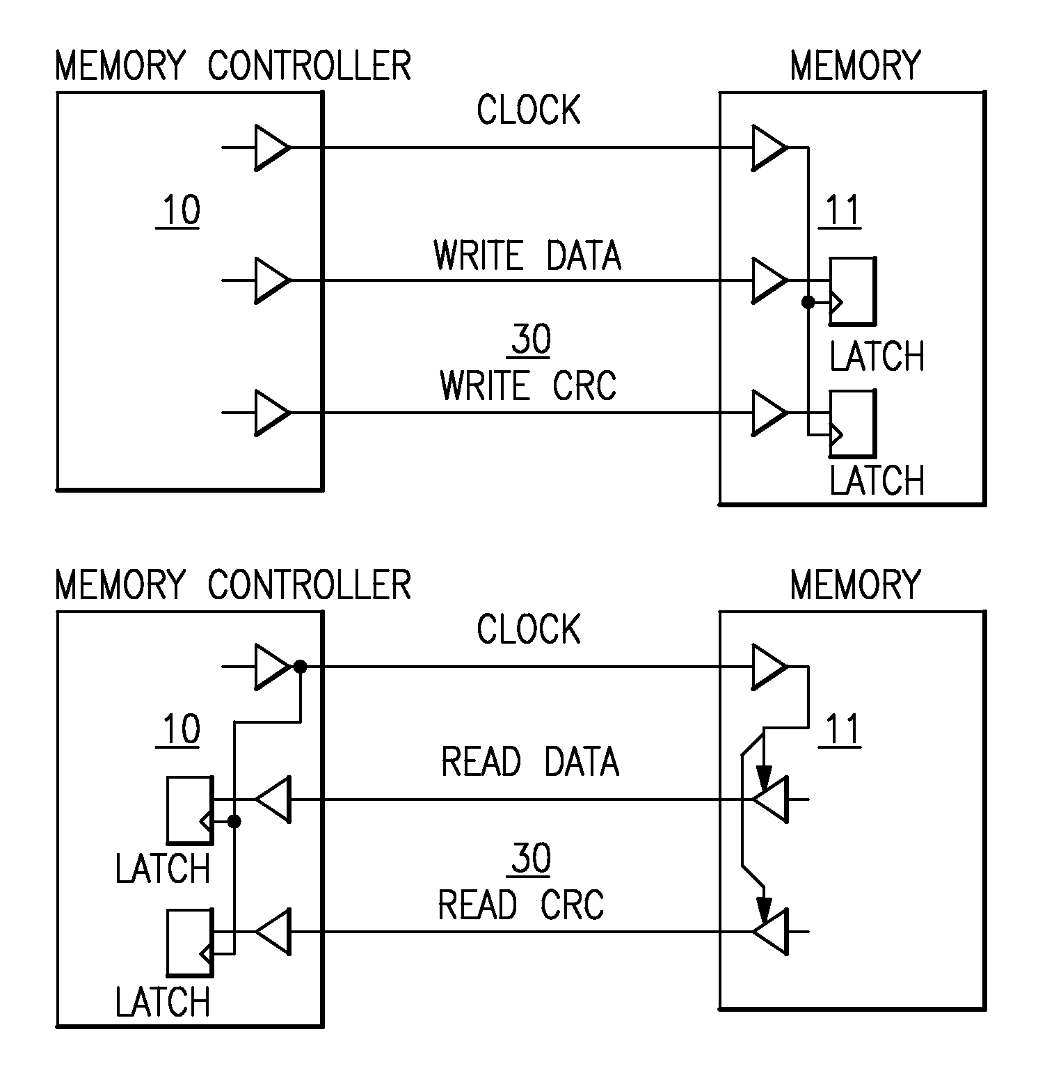
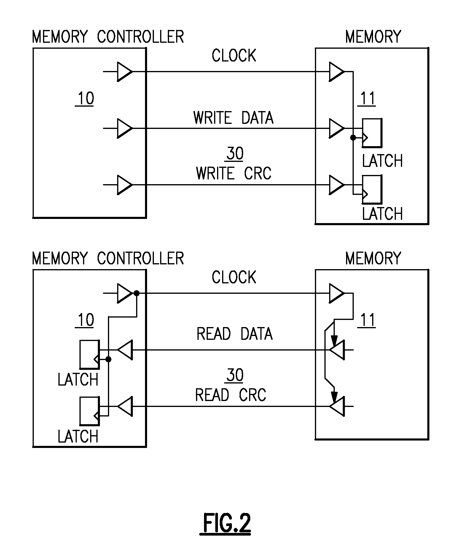
[0018]As see by FIG. 2 a memory controller 10 and a memory storage device (DRAM or DIMM of DRAMs) 11 which have a data communication bus 30 there between can...
PUM
 Abstract
Description
Claims
Application Information