Compound semiconductor device and the fabricating method of the same

a semiconductor and manufacturing method technology, applied in the direction of semiconductor devices, basic electric elements, electrical appliances, etc., can solve the problems of not being said to be sufficiently practical, reducing the output value by about 30%, and largely affecting the performance of the device, so as to achieve small deviation in characteristics, high reliability, and small degradation

Active Publication Date: 2009-12-29
FUJITSU LTD
View PDF21 Cites 14 Cited by
  • Summary
  • Abstract
  • Description
  • Claims
  • Application Information

AI Technical Summary

Benefits of technology

[0010]The present invention was made in views of the aforementioned problems and aims at providing a highly reliable compound semiconductor device which exhibits extremely small variations in the characteristics and small degradation with a lapse of time.

Problems solved by technology

However, in the case of using a GaN-HEMT as an electronic device having high withstand voltage, there is a problem that the characteristics thereof vary largely.
The reduction of the output value by about 30% after a lapse of 15 years can not be said to be sufficiently practical, and thus conventional GaN-HEMTs can be considered to have a significant problem in this regard.

Method used


Image

  • Compound semiconductor device and the fabricating method of the same
  • Compound semiconductor device and the fabricating method of the same
  • Compound semiconductor device and the fabricating method of the same

Examples


experiment 1

(1) Experiment 1

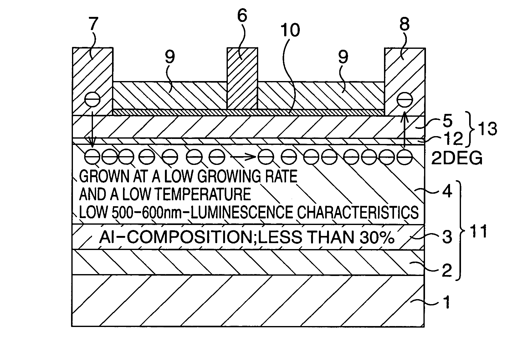
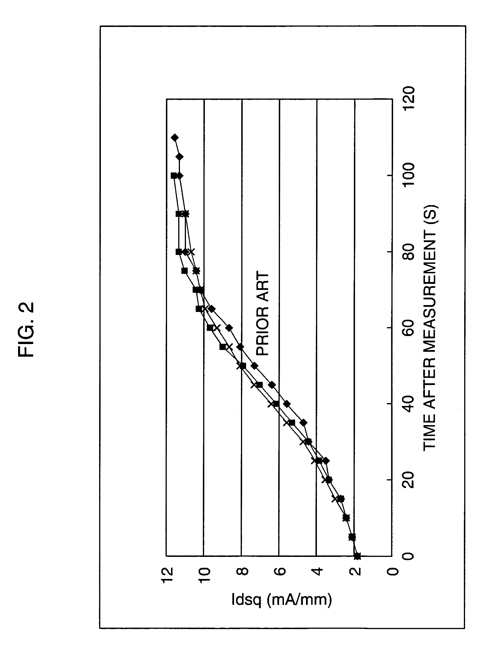
[0082]FIG. 8 illustrates monitored drain currents flowed at the instant of turning off the power-operation, in the GaN-HEMT according to the present embodiment. The horizontal axis represents the measuring time (second) and the vertical axis represents the drain current value (bias-point current: mA / mm) at the instant of turning off the power-operation of the GaN-HEMT. The number of measurements was three. In FIG. 8 there are also illustrated the results of measurements for the conventional GaN-HEMT of FIG. 2. At this time, while in the conventional GaN-HEMT the amount of Ga holes and the carbon concentration in the GaN layer serving as the electron transit layer were high values of 3×10¹⁸ / cm3 and 2×10¹⁸ / cm3, respectively, the amount of Ga holes and the carbon concentration in the GaN layer serving as the electron transit layer, in the GaN-HEMT according to the present embodiment, were 1×10¹⁴ / cm3 and 2×10¹⁴ / cm3, respectively, and these values are both lower compared ...


PUM


Abstract

A GaN layer functions as an electron transit layer and is formed to exhibit, at least at a portion thereof, A / B ratio of 0.2 or less obtained by a photoluminescence measurement, where “A” is the light-emission intensity in the 500-600 nm band, and “B” is the light-emission intensity at the GaN band-edge.

Description

CROSS-REFERENCE TO RELATED APPLICATIONS[0001]This application is based upon and claims the benefit of priority from the prior Japanese Patent Application No. 2004-332284, filed on Nov. 16, 2004, the entire contents of which are incorporated herein by reference.BACKGROUND OF THE INVENTION[0002]1. [Field of the Invention][0003]The present invention relates to a compound semiconductor device having a transistor configuration which includes a buffer layer containing GaN and the fabricating method of the same.[0004]2. [Description of the Related Art][0005]Amplifiers for the base-stations for recent portable phones are required to operate at high voltages and thus they must exhibit excellent withstand voltages. As electronic devices for achieving excellent withstand voltages, there have been actively developed compound semiconductor devices having a HEMT-configuration employing sapphire, SiC, GaN, Si or the like as a substrate, GaN as an electron transit layer and AlGaN as an electron sup...

Claims


Application Information

Patent Timeline
Patent Type & Authority Patents(United States)
IPC IPC(8): H01L29/778H01L21/205H01L21/338H01L29/812
CPCH01L21/0237H01L21/02378H01L21/02458H01L29/7787H01L21/0254H01L21/0262H01L21/02505H01L29/2003
Inventor KIKKAWA, TOSHIHIDEIMANISHI, KENJI
Owner FUJITSU LTD
Why Eureka
Try Eureka