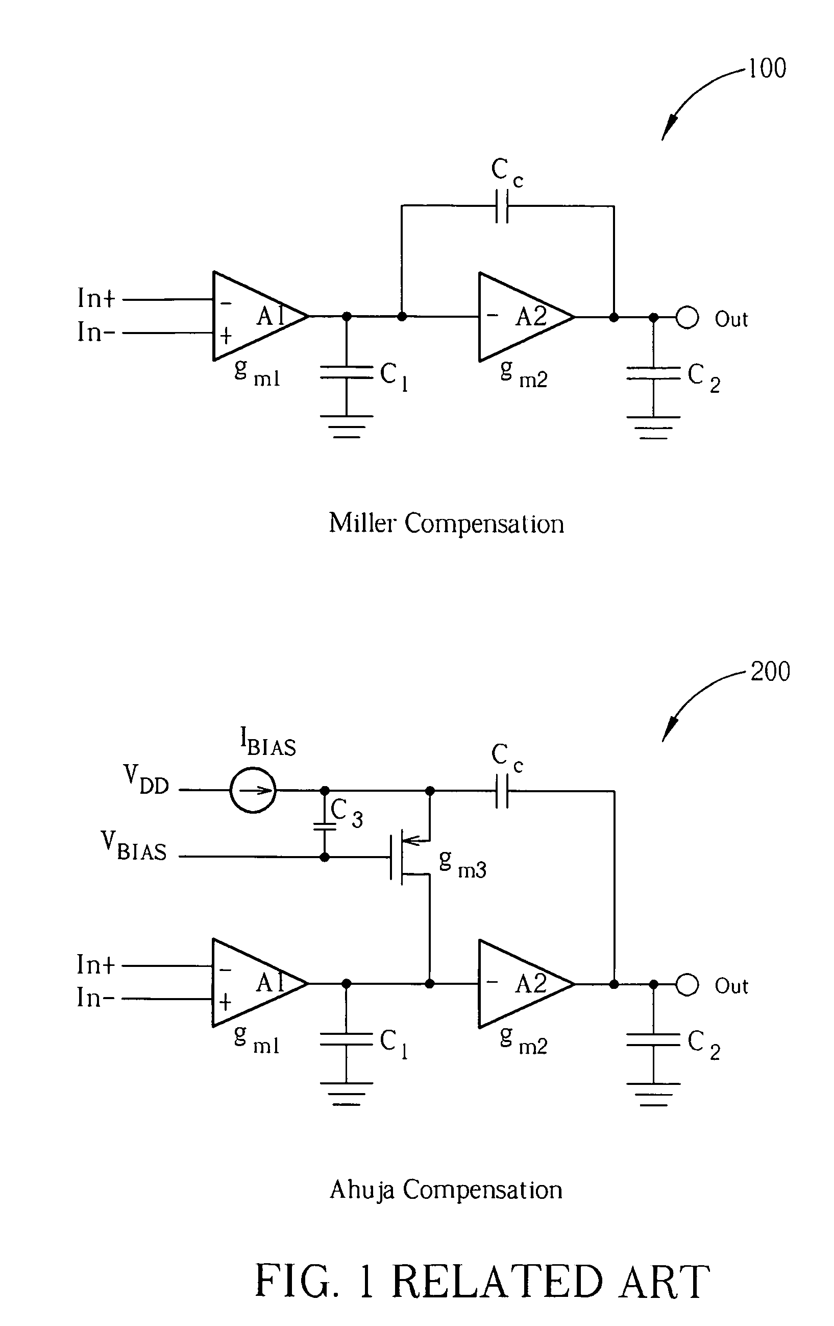
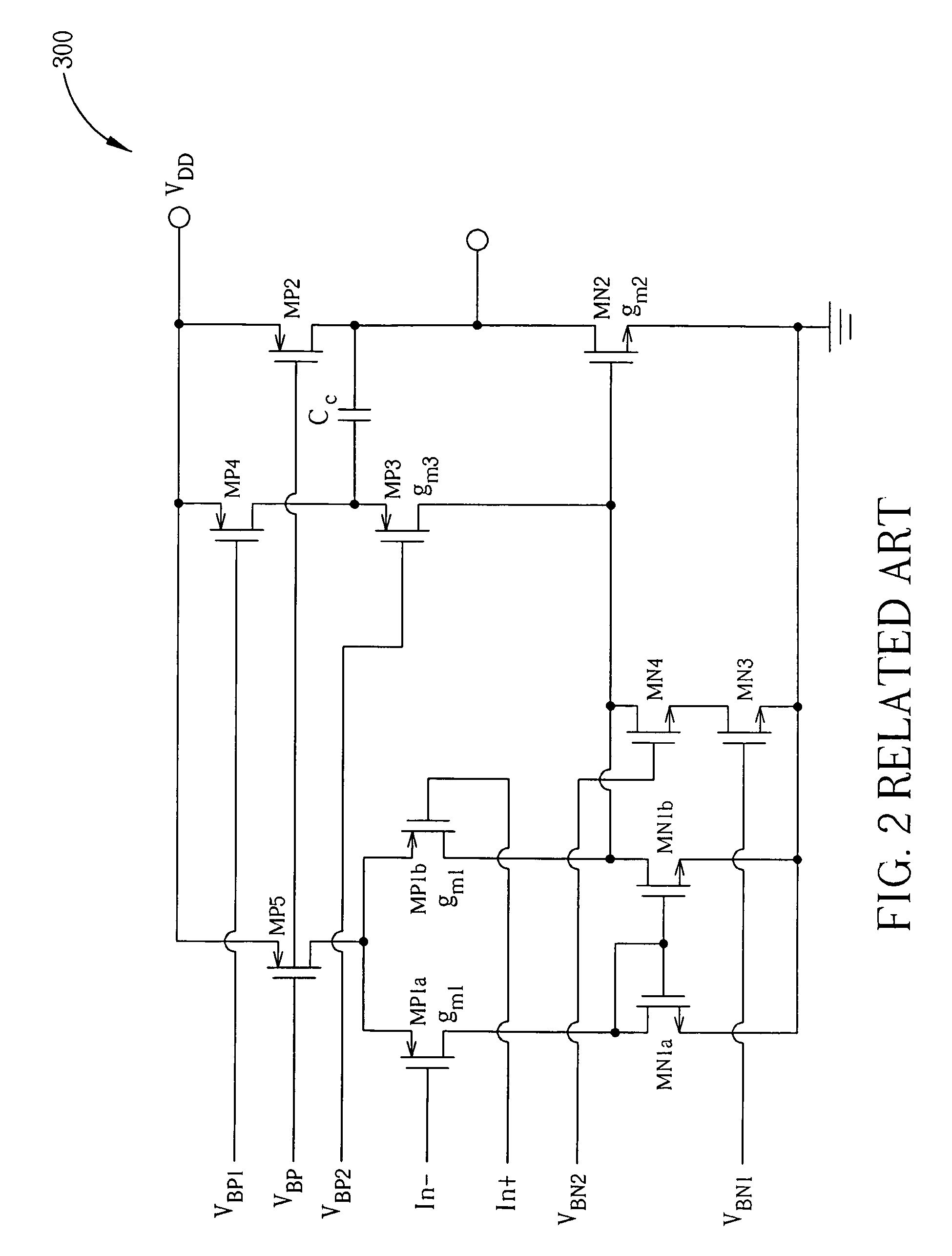
Ahuja compensation circuit for operational amplifier
a compensation circuit and amplifier technology, applied in amplifiers, amplifier modifications to extend bandwidth, electrical apparatus, etc., can solve the problems that the compensation scheme b>200/b> illustrated in fig. 1 does not achieve the desired
- Summary
- Abstract
- Description
- Claims
- Application Information
AI Technical Summary
Benefits of technology
Problems solved by technology
Method used
Image

Examples
Embodiment Construction
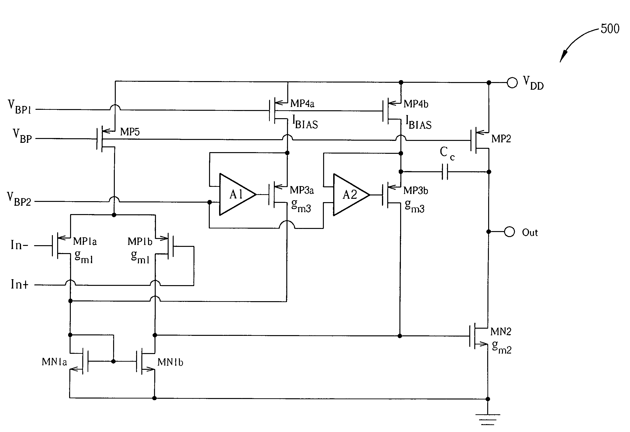
[0017]Please refer to FIG. 3. FIG. 3 is a diagram of an improved Ahuja compensation scheme 400. This scheme aims to improve the compensation offered by the original Ahuja compensation 200, by indirectly multiplying the transconductance of the compensating transistor MP3. The effect of this indirect multiplying is to move the non-dominant poles and zeros to higher frequencies and to increase damping for the non-dominant poles.
[0018]The improved scheme shown in FIG. 3 provides an amplifier A having a first input coupled to the bias current IBIAS, a second input coupled to the bias voltage VBIAS, and an output coupled to the gate of the compensating transistor MP3. The source voltage is therefore amplified, and this amplified voltage is then applied to the gate of the compensating transistor MP3. If the amplifier A has a gain of −A and the source voltage is vs, then the gate-source voltage vgs is equal to −(1+A) vs. The gate-source voltage has therefore been multiplied by a factor of (...
PUM
 Abstract
Description
Claims
Application Information
 - R&D
- Intellectual Property
- Life Sciences
- Materials
- Tech Scout
- Unparalleled Data Quality
- Higher Quality Content
- 60% Fewer Hallucinations
Browse by: Latest US Patents, China's latest patents, Technical Efficacy Thesaurus, Application Domain, Technology Topic, Popular Technical Reports.
© 2025 PatSnap. All rights reserved.Legal|Privacy policy|Modern Slavery Act Transparency Statement|Sitemap|About US| Contact US: help@patsnap.com