Scan flip-flop with internal latency for scan input

a flip-flop and scan input technology, applied in the field of digital circuits, can solve problems such as set-up-time violations, hold-time violations, and difficulty in ensuring that no setup-time or hold-time violations occur

Inactive Publication Date: 2010-01-19
CHRONOCLOUD MEDTECH (SHANGHAI) CO LTD
View PDF12 Cites 37 Cited by
  • Summary
  • Abstract
  • Description
  • Claims
  • Application Information

AI Technical Summary

Benefits of technology

[0012]According to another aspect of the present invention, there is provided a method of operating a scan flip-flop circuit which includes a data signal input for receiving a data signal, a scan input for receiving a scan signal and a clock input for receiving a clock signal. The method includes receiving a scan signal at the scan input, and receiving a clock signal at the clock input. In addition, the method includes providing the data signal input and the scan signal input to a multiplexer; providing the clock signal to a flip-flop; and selecting the scan signal using the multiplexer for presentation at an input of the flip-flop. The method includes introducing a delay in the multiplexer along a signal path of the scan signal from the scan input to the flip flop, that is sufficient to allow sampling of the scan signal at the flip-flop on an edge of the clock signal, in the absence of any additional delays in the signal path of the scan signal; and providing an output of the flip-flop as an output signal of the circuit.

Problems solved by technology

If the input signal level is sampled before the setup-time, a setup-time violation occurs.
Similarly, if the input signal changes before the required minimum duration following the clock edge used for sampling, a hold-time violation occurs.
As can be appreciated, in high speed circuits utilizing a clock signal with high frequency, it is often challenging to ensure that no setup-time or hold-time violations occur.
Hold violations often occur in pipeline stages of a circuit that have no combinatorial logic between them.
Scan flip-flops so operated have no combinatorial logic connected between them, and signals propagate from one stage to another very quickly, potentially causing hold-time violations.
Unfortunately, inserting buffers causes the area required by the resulting integrated circuit to increase, thereby increasing costs.

Method used


Image

  • Scan flip-flop with internal latency for scan input
  • Scan flip-flop with internal latency for scan input
  • Scan flip-flop with internal latency for scan input

Examples


Embodiment Construction

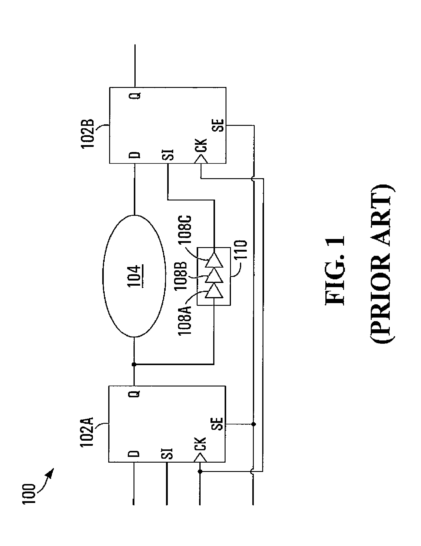
[0028]FIG. 1 depicts a simplified schematic diagram of an integrated circuit 100 with conventional scan flip-flops 102A, 102B (individually and collectively scan flip-flops 102), a combinatorial block 104, and buffers 108A, 108B, 108C (individually and collectively delay buffers 108). As depicted, each scan flip-flop 102A, 102B has a normal or functional data input (D), a scan input (SI), as well as clock input (CK). The output of scan flip-flop 102A may be interconnected to a combinatorial block 104 which further interconnects another scan flip-flop 102B. In case of a non-ideal clock distribution, there may be a skew between clock signals supplied to scan flip-flops 102A and 102B. As will become apparent, delay buffers 108 are inserted to introduce propagation delay in some signal paths, to help meet timing requirements.

[0029]Testing is important in the manufacturing of integrated circuits. While simulations are used to verify the design of a circuit such as circuit 100, manufactur...


PUM


Abstract

A scan flip-flop circuit including a data input, a scan input, a data output, a flip-flop, a multiplexer and a delay element is provided. The multiplexer allows selection of either the scan input or the data input for presentation at the input of the flip-flop. The flip-flop provides an output signal at the output of the scan flip-flop. The delay element is in a signal path between the scan input and the input of the flip-flop, and provides a signal propagation delay between the scan input and the input of the flip-flop. The delay between the scan input and the input of the flip-flop is substantially larger than the signal propagation delay between the data input and the input of the flip-flop. The delay in the scan path reduces the need for external buffers to avoid hold-time violations during scan testing of integrated circuits.

Description

FIELD OF THE INVENTION[0001]The present invention relates generally to digital circuits, and more particularly to scan flip-flops.BACKGROUND OF THE INVENTION[0002]Digital circuits play an increasingly important role in a variety of devices such as digital cameras, cellular telephones, digital music players and digital video disk (DVD) players, portable computing devices and digital television sets.[0003]Further proliferation of digital devices will be aided by continued decreasing costs, as exemplified by the increasing density of transistors packed on to a given area of silicon die. Reducing the area consumed by an integrated circuit (IC) formed on a silicon die is thus an important factor in lowering costs. Moreover, smaller die sizes are desirable as they increase the yield from a given silicon wafer. Performance is also typically increased as electrical interconnections between various blocks in the integrated circuit are shortened.[0004]Flip-flops are among the basic building b...

Claims


Application Information

Patent Timeline
Patent Type & Authority Patents(United States)
IPC IPC(8): H03K3/289H03K3/356
CPCG01R31/318536G01R31/31858
Inventor AHMADI, RUBIL
Owner CHRONOCLOUD MEDTECH (SHANGHAI) CO LTD
Why Eureka
Try Eureka