Semiconductor memory device and system providing spare memory locations

a memory device and semiconductor technology, applied in the field of semiconductor memory devices and, can solve the problems of memory data error rate increase, memory defects within individual memory devices, and memory errors that may still be encountered during normal use of devices,

Inactive Publication Date: 2010-02-02
HEWLETT-PACKARD ENTERPRISE DEV LP
View PDF21 Cites 55 Cited by
  • Summary
  • Abstract
  • Description
  • Claims
  • Application Information

AI Technical Summary

Problems solved by technology

However, increasing memory data error rates often accompany these advancements.
More specifically, both “hard errors” (permanent defects in a memory device, such as one or more defective memory cells) and “soft errors” (data errors of a temporary nature, such as inversion of data held within one or more memory cells) tend to become more prevalent with each new technology generation.
Some of these memory defects within individual memory devices are discovered during the manufacturing process by way of test equipment writing multiple data patterns to each of the device memory locations, reading the data back, and comparing the data read with the data written.
However, after the memory device is then placed in an operating computer system, both hard and soft errors may still be encountered during normal use of the device.
Typically, the more EDC data being utilized, the higher the number of errors being detected and corrected, but also the higher the amount of memory capacity overhead incurred.
However, similar to the use of EDC, the use of spare devices also increases the cost and memory overhead associated with the memory system.
Even with these advanced memory protection mechanisms, further memory technological advances often involve attendant increases in hard and soft errors rates, thus reducing device reliability.
Thus, such advances in memory technology may have the unintended effect of reducing the effectiveness of the EDC and related schemes currently employed in computer memory systems.

Method used


Image

  • Semiconductor memory device and system providing spare memory locations
  • Semiconductor memory device and system providing spare memory locations
  • Semiconductor memory device and system providing spare memory locations

Examples


Embodiment Construction

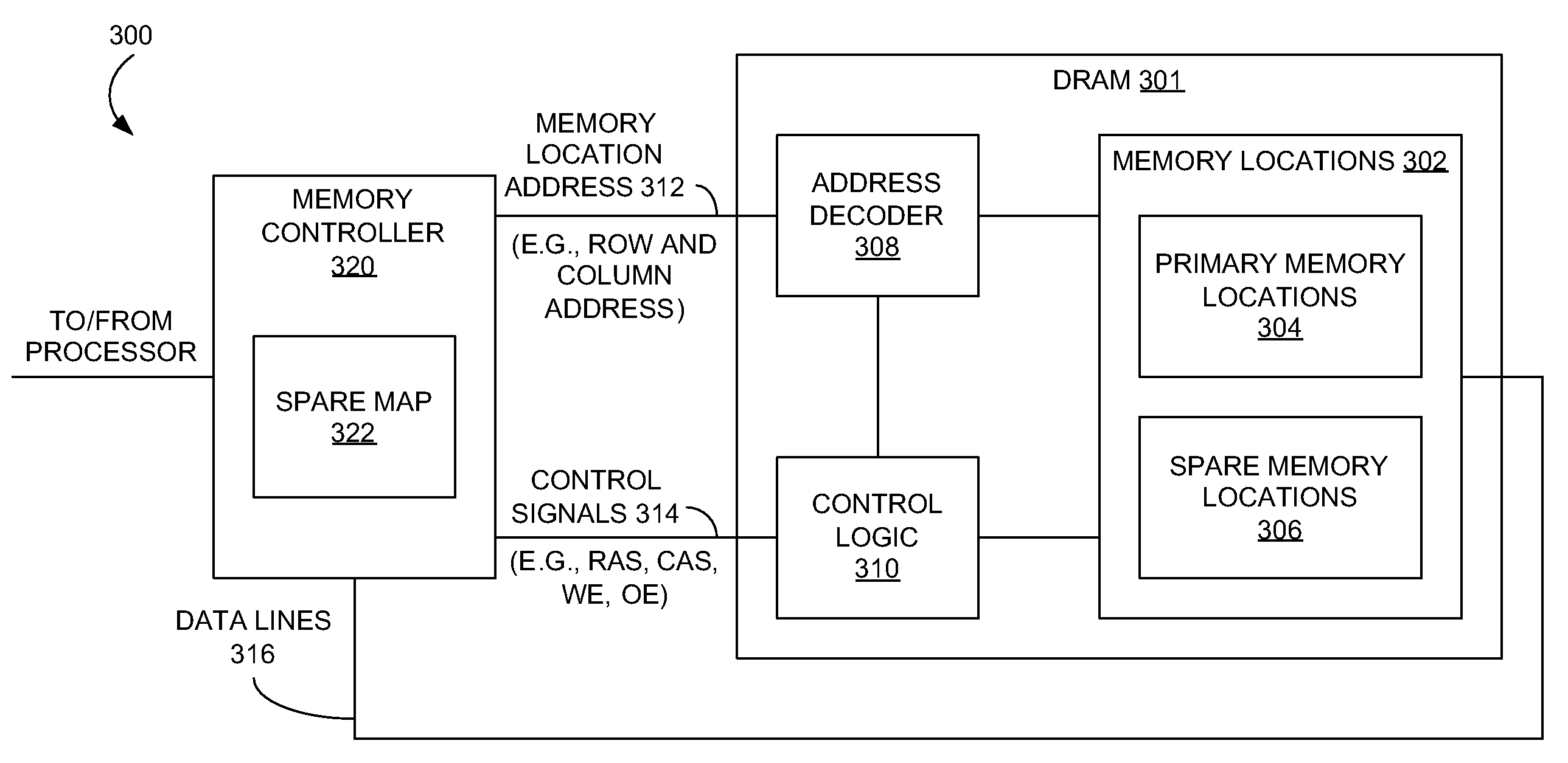
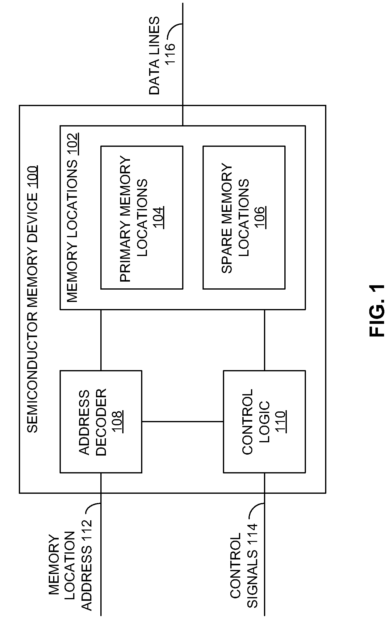
[0012]FIG. 1 provides a block diagram of one embodiment of the invention: a semiconductor memory device 100 that includes a plurality of memory locations 102. More specifically, the memory locations 102 include a plurality of primary memory locations 104 and a plurality of spare memory locations 106. Included in the device 100 is an address decoder 108 configured to receive a memory location address 112 and process the address 112 to select one of the memory locations 102. Also provided is control logic 110 configured to receive control signals 114 and process the control signals 114 to determine whether the selected one of the memory locations 102 is one of the primary memory locations 104 or one of the spare memory locations 106. The control logic 110 is also configured to provide access to the selected one of the memory locations 102 via data lines 116. In another embodiment, a memory controller (not shown in FIG. 1) may be employed to generate the memory location address 112 and...


PUM


Abstract

A semiconductor memory device having a plurality of memory locations is presented. The plurality of memory locations includes a plurality of primary memory locations and a plurality of spare memory locations. The device includes an address decoder configured to receive a memory location address and process the address to select one of the memory locations. The device further includes control logic configured to receive control signals and process the control signals to determine whether the selected one of the memory locations is one of the primary memory locations or one of the spare memory locations, and to provide access to the selected one of the memory locations via data lines.

Description

BACKGROUND OF THE INVENTION[0001]A vital component of virtually all computer systems is a semiconductor or solid-state memory system. Such memory often holds both the programming instructions for a processor of the computer system, as well as the data upon which those instructions are executed. In one example, the memory system may include one or more dual in-line memory modules (DIMMs), with each DIMM carrying multiple dynamic random access memory (DRAM) integrated circuits (ICs). Other memory technologies, such as static random access memories (SRAMs), and other memory organizational structures, such as single in-line memory modules (SIMMs), are also employed in a variety of computer systems. In addition, one or more processors may be coupled with the memory modules through a memory controller, which translates data requests from the processor into accesses to the data held in the memory modules.[0002]Computer systems have benefited from the ongoing advances made in both the speed...

Claims


Application Information

Patent Timeline
Patent Type & Authority Patents(United States)
IPC IPC(8): G11C29/00
CPCG11C8/20G11C29/70G11C29/76
Inventor THAYER, LARRY J.
Owner HEWLETT-PACKARD ENTERPRISE DEV LP
Why Eureka
Try Eureka