Die rearrangement package structure using layout process to form a compliant configuration

a package structure and layout technology, applied in the direction of semiconductor devices, semiconductor/solid-state device details, electrical devices, etc., can solve the problems of signal coupling and noise, the reliability of the package may be reduced, and the wlp aforementioned may not meet the design of smaller dies, so as to increase yield and reliability

Active Publication Date: 2010-02-16
CHIPMOS TECH INC
View PDF18 Cites 62 Cited by
  • Summary
  • Abstract
  • Description
  • Claims
  • Application Information

AI Technical Summary

Benefits of technology

[0009]According to the problems described above, the object of the present invention is to provide a dice rearrangement package structure with the alignment mark and the package method package structure. Thus, the main object of the present invention is to provide a B-stage material to encapsulate the dice to increase the yield and the reliability.
[0010]Another object of the present invention is to provide the packaging method for dies rearrangement. The dies derived from a 12-inches wafer are rearranged on the substrate of an 8-inches wafer. The packaging equipments for the 8-inches wafer may be utilized to reduce the packaging cost.
[0011]Another object of the present invention is to provide the packaging method of dies rearrangement. All of dies packaged are known good ones to reduce the packaging and manufacturing costs.

Problems solved by technology

However, for WLP, the increasing number and the reduced pitches of the bonding pads result in signal coupling and noise.
In addition, the reliability of package may be reduced because of the reduced pitches.
Thus, WLP aforementioned may not satisfy the design of smaller dies.
Because both the dies and the molding structure are thin very much, the stress from the molding structure itself would cause curl after the substrate is separated from the molding structure.
The curl of the molding structure may make a sequential saw process difficult.

Method used


Image

  • Die rearrangement package structure using layout process to form a compliant configuration
  • Die rearrangement package structure using layout process to form a compliant configuration
  • Die rearrangement package structure using layout process to form a compliant configuration

Examples


Embodiment Construction

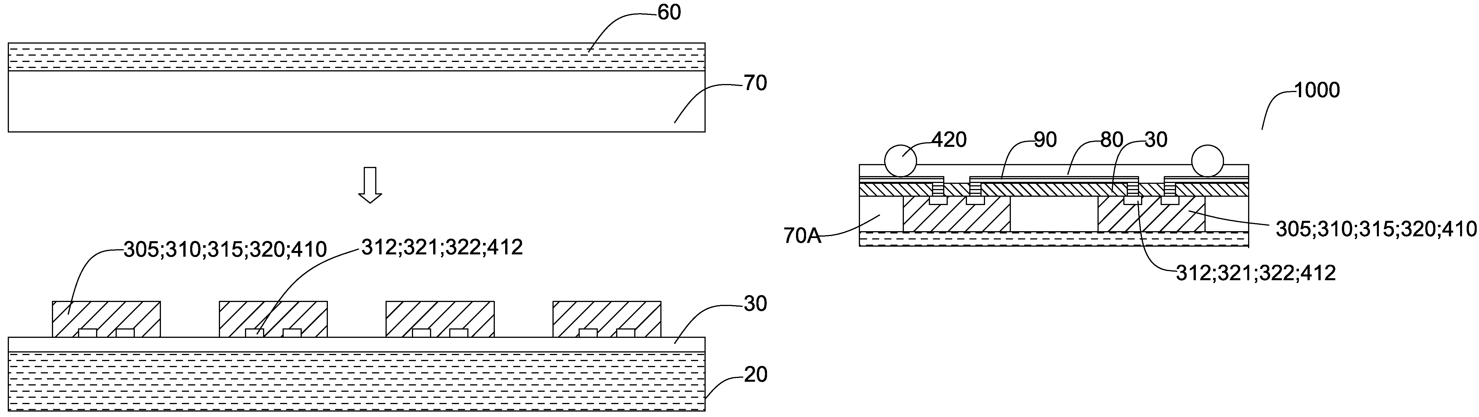
[0022]The present invention provides a packaging method for dies rearrangement to re-dispose dies on another substrate for packaging. Following illustrations describe detailed the process or steps for understanding the present invention. Obviously, the present invention is not limited to the embodiments of a stacked structure; however, the preferred embodiments of the present invention are illustrated as followings. Besides, the present invention may be applied to other embodiments, not limited to ones mentioned.

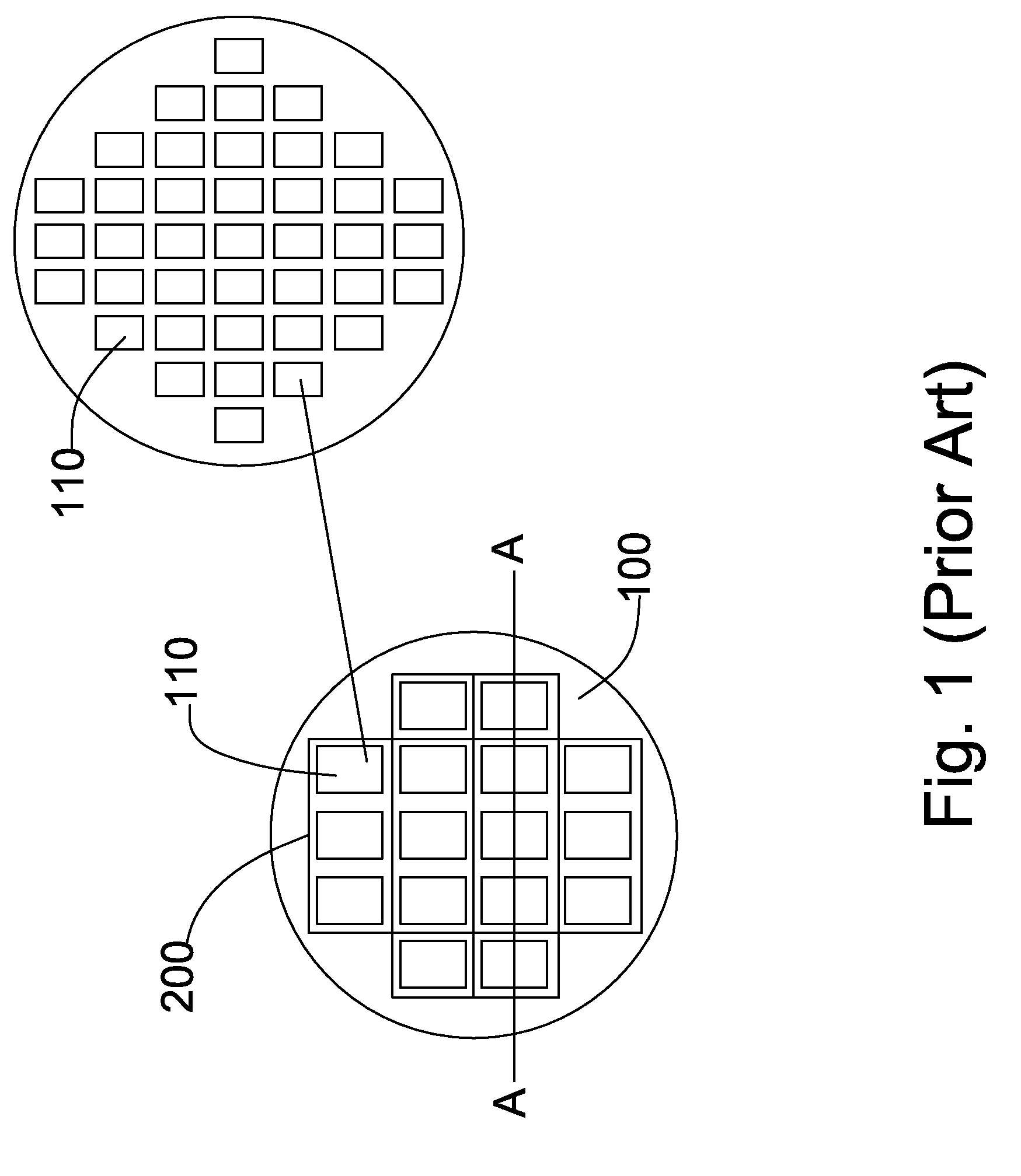
[0023]In modern semiconductor packaging process, a wafer which has been implemented by a front end process is done by a thinning process in thickness about 2 to 20 mil. A sawing process is applied on the wafer to form a plurality of dice 110 units. Then, these dies 110 are transferred from a pick and place to another substrate 100. Shown in FIG. 1, it is obvious that there are wider pitches among the dies 110 on the substrate 100 than the ones before sawing. Thus, these rear...


PUM


Abstract

A die rearrangement package structure is provided, which includes a die that having an active surface and a bottom surface, and a plurality of pads is disposed on the active surface; a package body is provided to cover a die and the active surface being exposed; a polymer material with at least one slit is provided to cover the active surface and the pads is exposed from said slits; one ends of a plurality of metal traces is electrically connected to each pads; a protective layer is provided to cover the active surface of the dies and each metal traces, and the other ends of the metal traces being exposed; a plurality of connecting elements is electrically connected other ends of the metal traces, the characterized in that: the package body is a B-stage material.

Description

BACKGROUND OF THE INVENTION[0001]1. Field of the Invention[0002]The present invention is related to a packaging method of semiconductor, more particularly, to a package method and a structure of dies rearrangement by a redistribution layer process to form a module with package body.[0003]2. Description of the Prior Art[0004]Miniaturized semiconductor dice has been a trend for its various functions. These semiconductor dies should be provided with more and more I / O pads within a smaller region, so the density of metal pins raises. Thus, the package technology of lead frame has been replaced by the technology of ball grid array (BGA). It is advantageous for BGA to provide more compact density and have solder less subject to damage and distorted.[0005]With 3C products in fashion, such as cell phone, PDA or iPod, these 3C products are equipped with at least one systemic chip within a smaller volume. A wafer level package (WLP) has been developed to packaging a wafer before sawing. U.S. ...

Claims


Application Information

Patent Timeline
Patent Type & Authority Patents(United States)
IPC IPC(8): H01L21/44H01L21/4763H01L21/48H01L21/50
CPCH01L21/568H01L23/5389H01L24/19H01L24/20H01L24/97H01L21/6835H01L24/25H01L2224/12105H01L23/3128H01L2221/68345H01L2221/68359H01L2224/04105H01L2224/20H01L2224/211H01L2224/97H01L2924/01015H01L2924/01075H01L2924/01082H01L2924/01094H01L2924/09701H01L2924/15311H01L2224/24137H01L2924/12041H01L2924/01005H01L2924/01006H01L2924/01033H01L2224/82H01L2224/92144H01L2924/3511
Inventor SHEN, GENG-SHIN
Owner CHIPMOS TECH INC
Why Eureka
Try Eureka