Semiconductor device

a semiconductor device and capacitor technology, applied in the field of semiconductor devices, can solve the problems of small shielding effect against leakage of electric field to the lower electrode, deterioration of dimensional accuracy, unstable capacitance value of capacitors, etc., and achieve the effect of improving dimensional accuracy and stable capacitance valu

Inactive Publication Date: 2010-02-16
RENESAS ELECTRONICS CORP
View PDF6 Cites 7 Cited by
  • Summary
  • Abstract
  • Description
  • Claims
  • Application Information

AI Technical Summary

Benefits of technology

[0011]Here, when the first electrode and the second electrode are formed, the shielding electrode may be simultaneously formed as the dummy pattern. Thereby, the dimensional accuracy of the semiconductor device may be improved. Moreover, the capacitance value of the MIM capacitor may be stabilized because the shielding electrode is formed in the outer edge of the layer in which the first electrode and the second electrode are formed, and the capacitor forming region may be shielded from other regions.
[0014]According to the present invention, the dimensional accuracy of a semiconductor device is improved, and a stable capacitance value is given in the semiconductor device including a capacitor with an MIM structure.

Problems solved by technology

However, when there are variations in an interconnection pattern at forming the multilayer interconnection structure, there is caused a problem that a flattened layer is not realized, and the dimensional accuracy is deteriorated.
Incidentally, a capacitor element has had a problem that the finer semiconductor device causes other interconnections formed in a surrounding region of the capacitor to have the influence on the device, and a capacitance value of the capacitor to become unstable.
H5-90489 has a problem that a shielding effect against a leakage electric field to the lower electrode is small, as the shields are arranged, respectively, at positions which are opposed to and apart from each side of the polygonal upper electrode.
Moreover, there is also a problem that dimensional accuracy at forming the lower electrode may not be improved.

Method used


Image

  • Semiconductor device
  • Semiconductor device
  • Semiconductor device

Examples


first embodiment

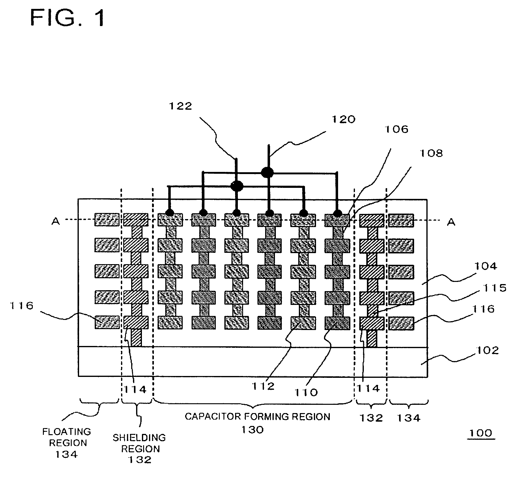
[0041]FIG. 1 is a cross-sectional view showing a configuration of a semiconductor device 100 according to an embodiment.

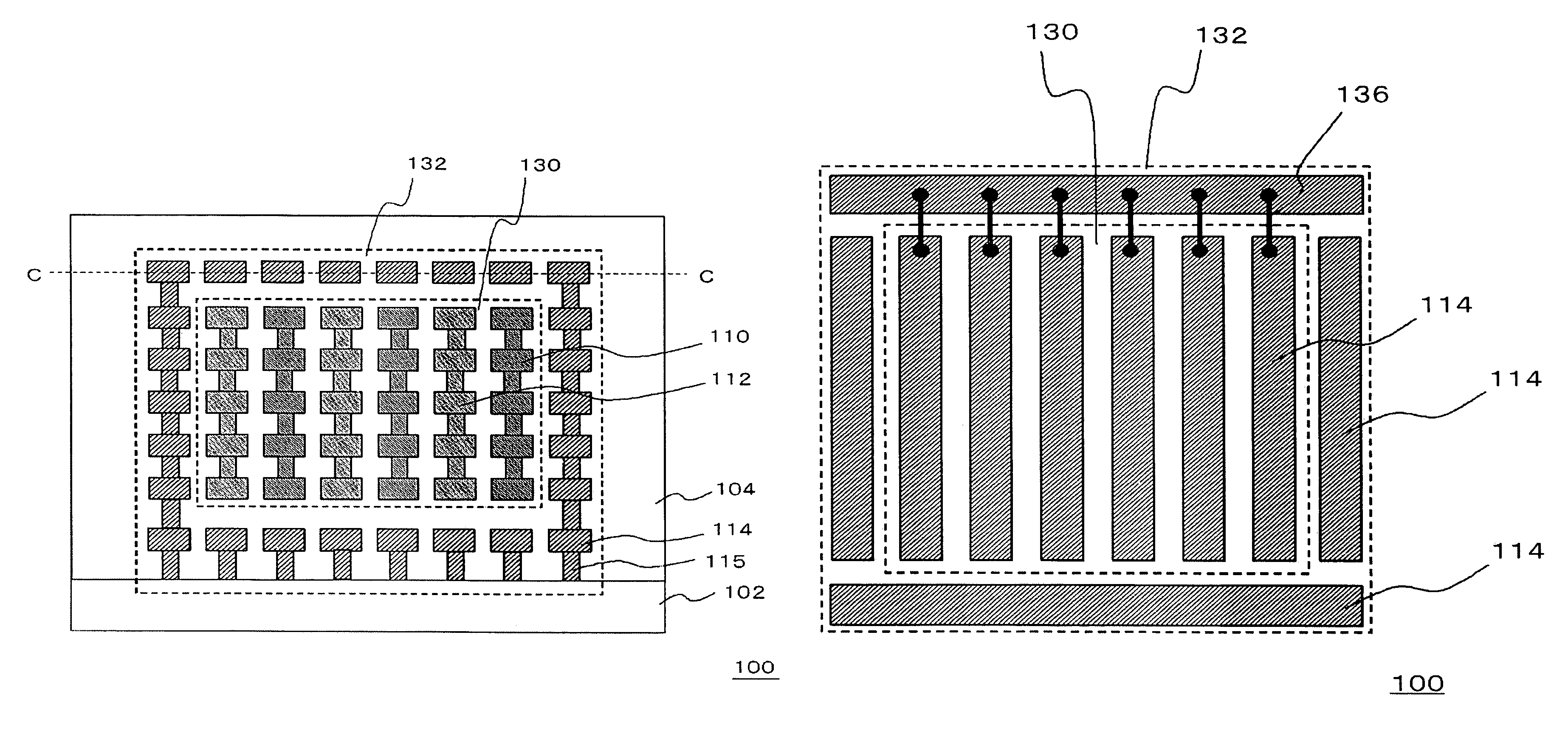
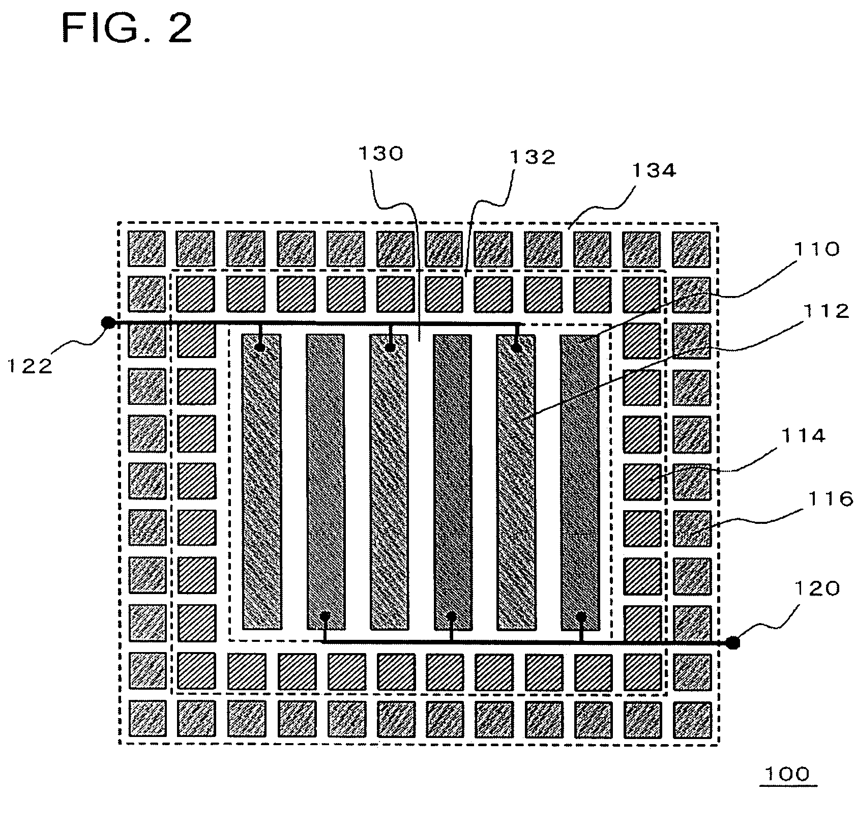
[0042]The semiconductor device 100 includes a semiconductor substrate 102, a capacitor forming region 130 in which an MIM capacitor is formed, and a shielding region 132 for shielding the capacitor forming region 130 from other regions.

[0043]The MIM capacitor includes an insulating interlayer 104 (insulating film) formed on the semiconductor substrate 102, a first electrode 110, and a second electrode 112. The first electrode 110 and the second electrode 112 are arranged facing each other through the insulating film 104.

[0044]The shielding region 132 includes a plurality of shielding electrodes 114 formed on the semiconductor substrate 102 in the outer edge of the capacitor forming region 130 to surround the capacitor forming region 130. The shielding electrodes 114 are formed in the same layer as that of the MIM capacitor. In this embodiment, the shielding electro...

second embodiment

[0082]FIG. 13 is a cross-sectional view showing a configuration of a semiconductor device 100 according to the embodiment.

[0083]The present embodiment differs from the first embodiment in a point that shielding electrodes 114 are not connected to a semiconductor substrate 102. Other points are similar to those of the first embodiment which have been explained, and the explanation will not be repeated. In the present embodiment, the shielding electrodes 114 are connected to a third potential line 138, and the potential of the shielding electrodes 114 is set according to a potential at which the third potential line 138 is set.

[0084]FIG. 14 is a cross-sectional plan view taken along the D-D line of the semiconductor device 100 shown in FIG. 13.

[0085]Although the floating electrodes 116 are not shown in the drawing, the semiconductor device 100 may include the floating electrodes 116 in this embodiment as well. In the present embodiment, the shielding electrodes 114 may have a similar ...

third embodiment

[0096]FIG. 17 is a cross-sectional view showing a configuration of a semiconductor device 100 according to an embodiment.

[0097]Although it is not shown, the semiconductor device 100 may include a logic region having a transistor formed in a region different from a capacitor forming region 130 on a semiconductor substrate 102, and a multilayer interconnection structure formed on the transistor in this embodiment as well. Interconnections and vias in the capacitor forming region 130, a shielding region 132, a floating region 134, and the like may be simultaneously formed with interconnections and vias in the multilayer interconnection structure of the logic region.

[0098]The present embodiment differs from the semiconductor device 100 according to the first and second embodiments in a point that a first electrode 110, an insulating interlayer 104, and a second electrode 112 are formed in different layers from one another.

[0099]The semiconductor device 100 according to the present embod...


PUM


Abstract

A semiconductor device includes a capacitor with an MIM structure, by which the dimensional accuracy of the device is improved, and a stable capacitance value is given. The semiconductor device 100 includes: a semiconductor substrate 102; a capacitor forming region 130 in which an MIM capacitor is formed, which has an insulating interlayer 104 formed on the semiconductor substrate 102, a first electrode 110, and a second electrode 112, and the first electrode 110 and the second electrode 112 are arranged facing each other through the insulating interlayer 104; and a shielding region 132 which includes a plurality of shielding electrodes 114 formed in the outer edge of the capacitor forming region 130 and, at the same time, set at a predetermined potential in the same layer as that of the MIM capacitor on the semiconductor substrate 102, and shields the capacitor forming region 130 from other regions.

Description

[0001]This application is based on Japanese Patent application NO. 2005-123462, the content of which is incorporated hereinto by reference.BACKGROUND[0002]1. Technical Field[0003]The present invention relates to a semiconductor device including a capacitor with a metal-insulator-metal (MIM) structure.[0004]2. Related Art[0005]Recently, an MIM capacitor, in which a parasitic resistance and parasitic capacitance are remarkably small in comparison with a conventional metal oxide semiconductor (MOS) capacitor, has been used more often for a capacitor element. Moreover, a one-chip structure in which such MIM capacitors are built into a logic device has been developed, too. In order to achieve the above structure, the structures and the manufacturing processes for both of the logic device and the capacitor device have been required to be integrated. A common logic device includes a multilayer structure in which interconnections are stacked to form a multi-layered structure. It is an impor...

Claims


Application Information

Patent Timeline
Patent Type & Authority Patents(United States)
IPC IPC(8): H01L29/00
CPCH01L23/5223H01L28/60H01L2924/0002H01L2924/00
Inventor KIKUTA, KUNIKOFURUMIYA, MASAYUKIYAMAMOTO, RYOTANAKAYAMA, MAKOTO
Owner RENESAS ELECTRONICS CORP
Why Eureka
Try Eureka