MOS resistance controlling device and MOS attenuator

a technology of mos resistance and control device, which is applied in the direction of pulse automatic control, pulse generator, pulse technique, etc., can solve the problems of affecting the variable attenuator, and achieve the effect of improving the precision of control of the mos resistan

Inactive Publication Date: 2010-02-16
KK TOSHIBA
View PDF12 Cites 15 Cited by
  • Summary
  • Abstract
  • Description
  • Claims
  • Application Information

AI Technical Summary

Benefits of technology

[0011]It is an object of the present invention to provide a MOS resistance controlling device to enhance the precision in control of the MOS resistance and a MOS attenuator having the MOS resistance controlling device.
[0013]In the MOS resistance controlling device according to the aspect, a plurality of MOS transistors are connected in series with one another and the output terminal of the operational amplifier is connected with the gates of the MOS transistors. Therefore, the input offset voltage of the operational amplifier is allotted to the MOS transistors, respectively so that the affection of the input offset voltage can be dispersed by the MOS transistors connected in series with one another. As a result, each MOS resistance of each MOS transistor can be controlled precisely.
[0015]The MOS attenuator utilizes the MOS resistance controlling device as described above. In this case, the output voltage of the MOS resistance controlling device is supplied so as to generate the MOS resistances of the ground MOS transistors in the attenuator. As a result, the MOS resistances of the ground MOS transistors can be controlled precisely so that the attenuation of the attenuator can be controlled as designed.
[0016]According to the aspects of the present inventions, the control precision in MOS resistance of the MOS resistance controlling device and the MOS attenuator can be enhanced.

Problems solved by technology

However, if the operational amplifier in the controlling circuit of the MOS resistance has a DC offset, the variable attenuator is affected by the DC offset of the operational amplifier.

Method used


Image

  • MOS resistance controlling device and MOS attenuator
  • MOS resistance controlling device and MOS attenuator
  • MOS resistance controlling device and MOS attenuator

Examples


Embodiment Construction

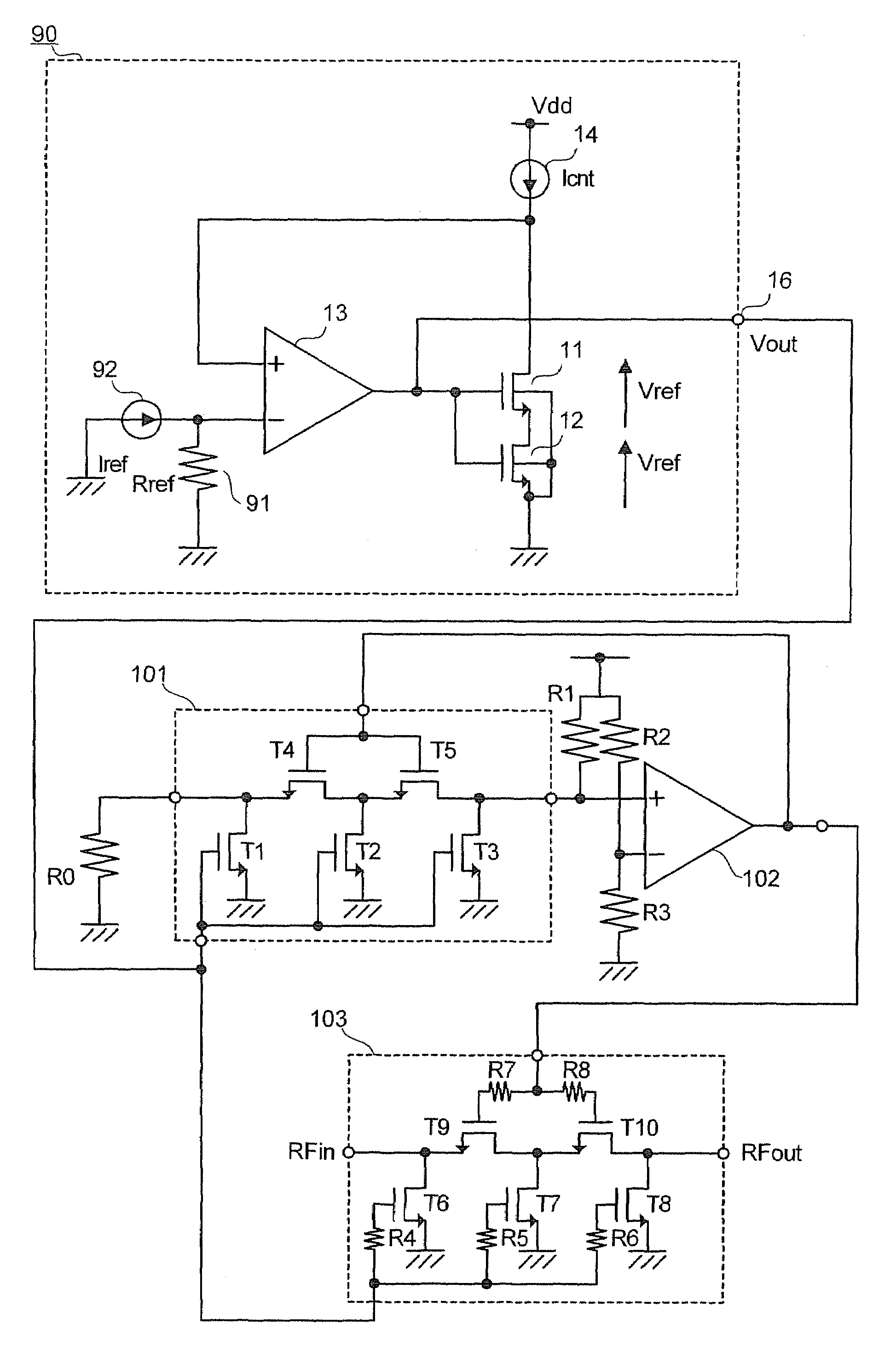
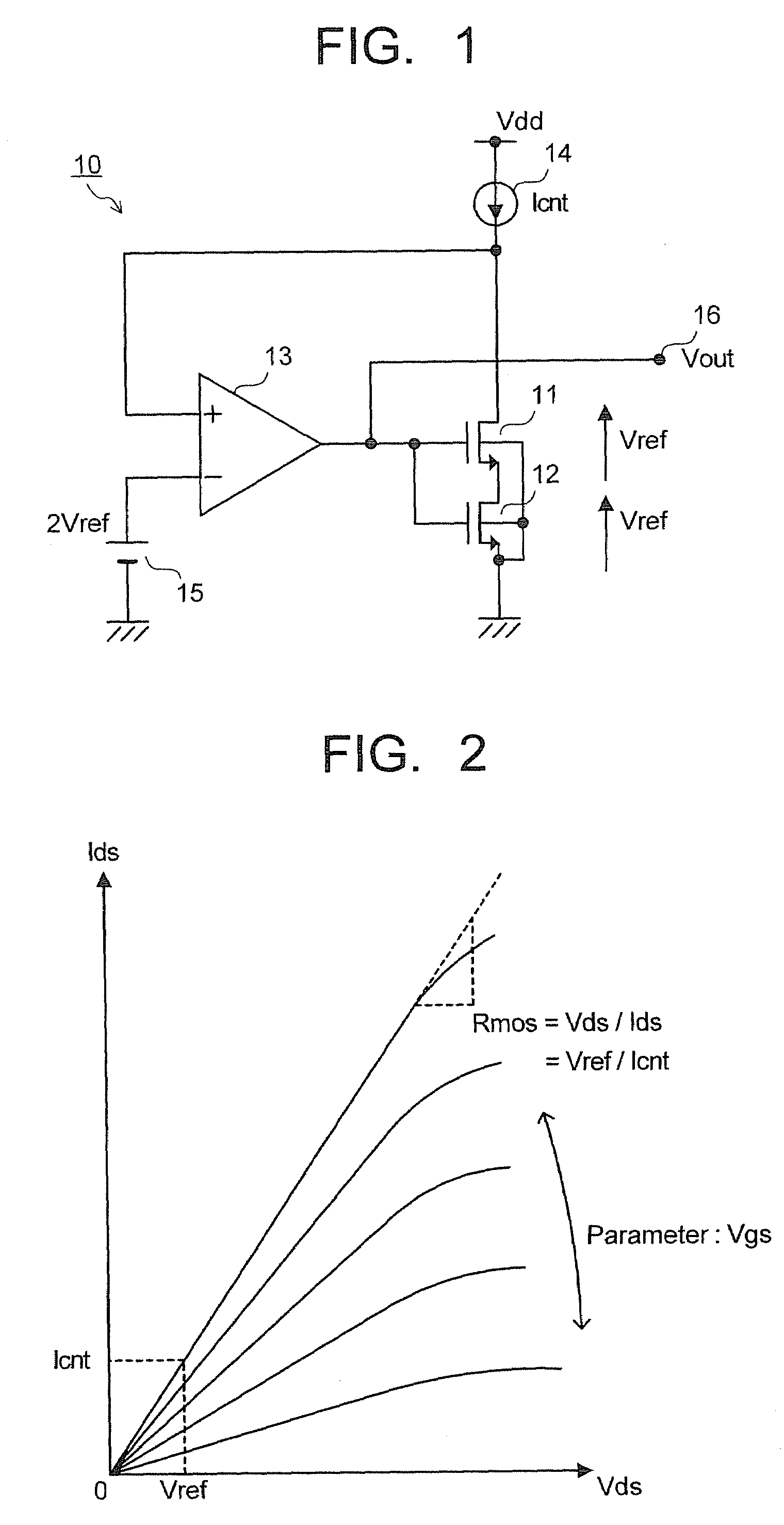
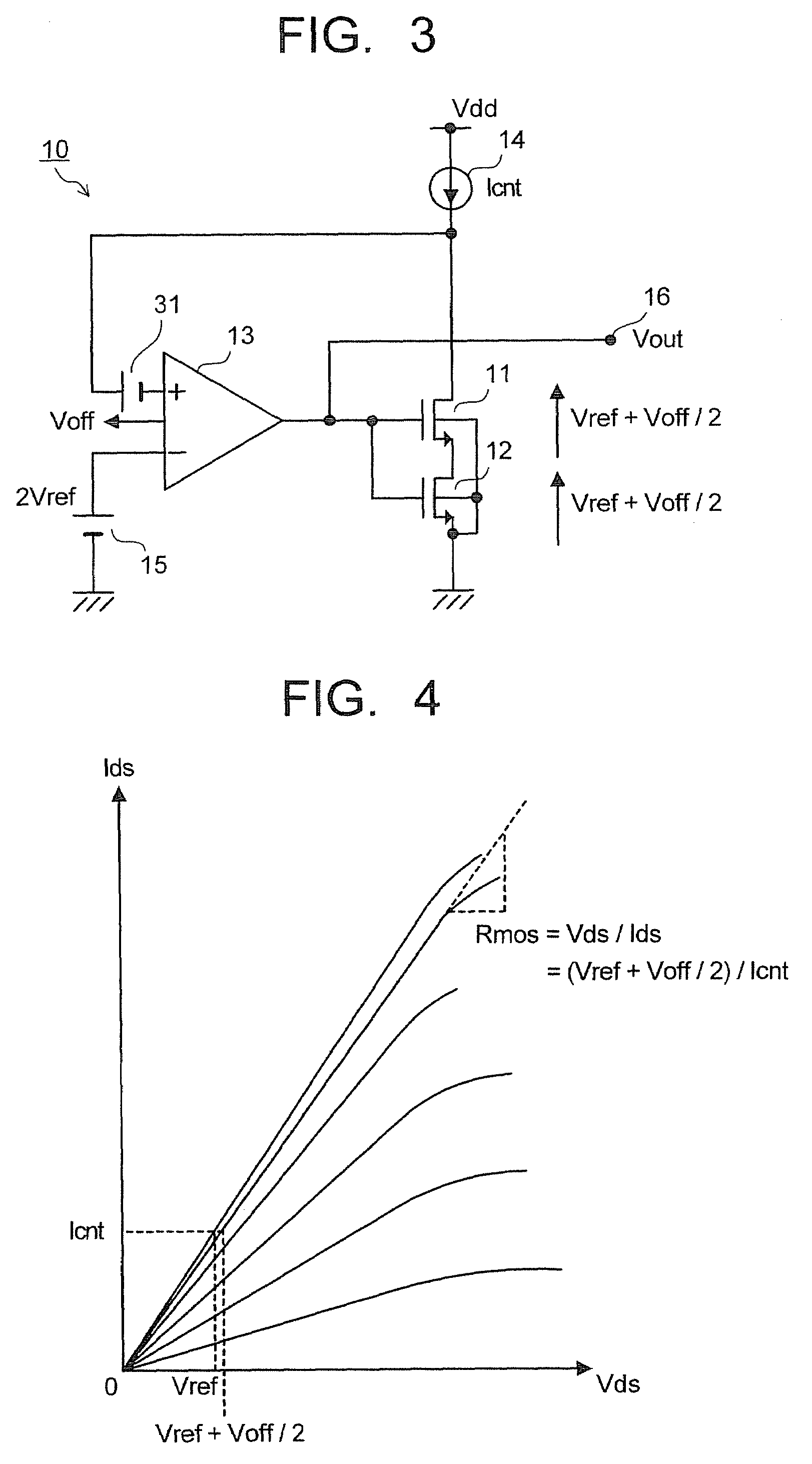
[0028]In an embodiment, the semiconductor area for a channel of each MOS transistor to be formed is electrically set to the first reference potential. Generally, the MOS transistor includes a semiconductor area (e.g., semiconductor substrate) for the channel to be formed. Therefore, if the first reference potential is set to the semiconductor area, the manufacturing process of a semiconductor device including the MOS transistors and the chip area of the semiconductor device can be reduced.

[0029]In another embodiment, the semiconductor area for a channel of each MOS transistor to be formed is electrically set to a source potential of each MOS transistor. In this case, the semiconductor area for the channel of each MOS transistor to be formed is set to the source potential thereof so that the fluctuation in characteristic (e.g., threshold value) between the MOS transistors due to the substrate effect can be prevented and thus, the output voltage can be generated at the output terminal...


PUM


Abstract

A MOS resistance controlling device includes: a plurality of MOS transistors having a first MOS transistor to N-th (the integer N is larger than 1) MOS transistor being serially connected, the source of the first MOS transistor being set to a first reference potential, the drain the N-th MOS transistor being set to a second reference potential, and the drain of an I-th MOS transistor being connected to the source of an I+1-th MOS transistor, where I is an integer from 1 to N−1; a current source which is electrically disposed at connection node between the drain of the N-th MOS transistors and the second reference potential; and an operational amplifier having a first input terminal being supplied with a third reference potential, a second input terminal connected with the connection node and an output terminal being connected with gates of the MOS transistors.

Description

CROSS-REFERENCE TO RELATED APPLICATIONS[0001]This application is based upon and claims the benefit of priority from the prior Japanese Patent Application No. 2006-303775, filed on Nov. 9, 2006; the entire contents of which are incorporated herein by reference.BACKGROUND OF THE INVENTION[0002]1. Field of the Invention[0003]The present invention relates to a MOS resistance controlling device for controlling the resistance between the source and drain of a MOS transistor and a MOS attenuator having the MOS resistance controlling device.[0004]2. Description of the Related Art[0005]A MOS transistor is widely available as a resistance element for various electronic circuits. In this case, the linear region of the MOS transistor is utilized. In the linear region of the MOS transistor, the resistance “Rmos” between the drain and source of the MOS transistor can be approximately represented by the equation of Rmos≈1 / {β·(Vgs−Vth)}. Herein, β=(μn·Cox)·(W / L) (μn: electron mobility, Cox: gate ox...

Claims


Application Information

Patent Timeline
Patent Type & Authority Patents(United States)
IPC IPC(8): H03L5/00
CPCH01L27/0802H03H11/245
Inventor ARAKI, YUTAOTAKA, SHOJIHASHIMOTO, TORU
Owner KK TOSHIBA
Why Eureka
Try Eureka