

Method and system for providing a magnetic element having a current confined layer
- Summary
- Abstract
- Description
- Claims
- Application Information
AI Technical Summary
Benefits of technology
Problems solved by technology
Method used
Image

Examples
first embodiment
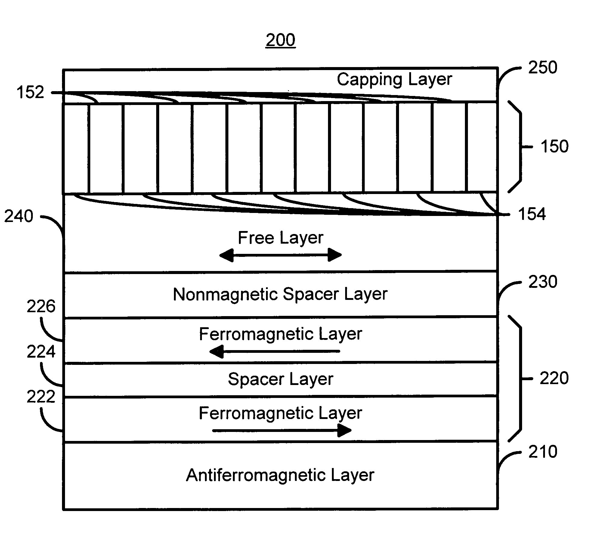
[0029]FIGS. 4A-4H depict embodiments of magnetic elements incorporating embodiments of the CCL 150 that is formed by sputtering. FIG. 4A is a diagram of a magnetic element 200 containing a sputtered CCL 150 in accordance with the present invention. The magnetic element 200 includes an AFM layer 210, a pinned layer 220, a nonmagnetic spacer layer 230, a free layer 240, the CCL 150 and an optional capping layer 250. In addition, seed layers (not shown) and lead layers (not shown) are generally also used. For a CPP configuration, the leads would be at the top, above the capping layer 250 and the bottom, below the AFM layer 210 and any seed layers.
[0030]In the embodiment shown, the synthetic pinned layer 220 includes ferromagnetic layers 222 and 226 separated by a conductive, nonmagnetic spacer layer 224. However, in an alternate embodiment, a simple pinned layer 220 could also be used. The ferromagnetic layers 222 and 226 are preferably CoFe, while the spacer layer 224 is preferably Ru...
second embodiment
[0032]FIG. 4B is a diagram of a magnetic element 300 containing a sputtered CCL in accordance with the present invention. The magnetic element 300 includes an AFM layer 310, a pinned layer 320, a nonmagnetic spacer layer 230, a free layer 340, the CCL 150 and an optional capping layer 350. In addition, seed layers (not shown) and lead layers (not shown) are generally also used. For a CPP configuration, the leads would be at the top, above the capping layer 350 and the bottom, below the AFM layer 310 and any seed layers.
[0033]In the embodiment shown, the synthetic pinned layer 320 includes ferromagnetic layers 322 and 326 separated by a conductive, nonmagnetic spacer layer 324. However, in an alternate embodiment, a simple pinned layer 320 could also be used. The ferromagnetic layers 322 and 326 are preferably CoFe, while the spacer layer 324 is preferably Ru. The spacer layer 324 is configured to ensure that the ferromagnetic layers 322 and 326 are antiferromagnetically coupled. The...
third embodiment
[0035]FIG. 4C is a diagram of a magnetic element 400 containing a sputtered CCL 150 in accordance with the present invention. The magnetic element 400 includes an AFM layer 410, a pinned layer 420, a nonmagnetic spacer layer 430, a free layer 440, the CCL 150 and an optional capping layer 450. In addition, seed layers (not shown) and lead layers (not shown) are generally also used. For a CPP configuration, the leads would be at the top, above the capping layer 450 and the bottom, below the AFM layer 410 and any seed layers.
[0036]In the embodiment shown, the synthetic pinned layer 420 includes ferromagnetic layers 422 and 426 separated by a conductive, nonmagnetic spacer layer 424. However, in an alternate embodiment, a simple pinned layer 420 could also be used. The ferromagnetic layers 422 and 426 are preferably CoFe, while the spacer layer 424 is preferably Ru. The spacer layer 424 is configured to ensure that the ferromagnetic layers 422 and 426 are antiferromagnetically coupled....
PUM
 Abstract
Description
Claims
Application Information