Organic el display apparatus and active matrix substrate

Inactive Publication Date: 2019-04-25
SHARP KK
View PDF3 Cites 1 Cited by
  • Summary
  • Abstract
  • Description
  • Claims
  • Application Information

AI Technical Summary

Benefits of technology

[0012]The emission intensity of each pixel is directly controlled by the drive TFT. Therefore, variations in the TFT characteristics of the drive TFT result in variations in emission intensity, leading to defective display quality su

Problems solved by technology

Therefore, variations in the TFT characteristics of the drive TFT result in variations in emi

Method used


Image

  • Organic el display apparatus and active matrix substrate
  • Organic el display apparatus and active matrix substrate
  • Organic el display apparatus and active matrix substrate

Examples


Example

First Embodiment

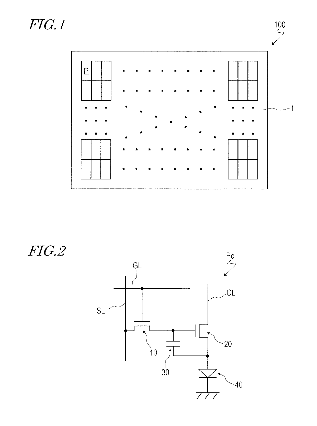
[0049]An organic EL display apparatus 100 according to this embodiment will be described with reference to FIG. 1. FIG. 1 is a plan view schematically showing the organic EL display apparatus 100.

[0050]As shown in FIG. 1, the organic EL display apparatus 100 has a plurality of pixels P arranged in a matrix. The pixels P typically include red pixels for displaying red, green pixels for displaying green, and blue pixels for displaying blue.

[0051]The organic EL display apparatus 100 also includes a substrate 1, and pixel circuits (not shown in FIG. 1), one for each pixel P. FIG. 2 shows an example pixel circuit.

[0052]The pixel circuit Pc of FIG. 2 includes a selection TFT 10, a drive TFT 20, and a capacitive element (storage capacitor) 30. The selection TFT 10 and the drive TFT 20 are supported by the substrate 1, and are each an oxide semiconductor TFT having an oxide semiconductor layer.

[0053]The gate electrode of the selection TFT 10 is connected to a gate line GL. T...

Example

Second Embodiment

[0116]In the first embodiment, the organic EL display apparatus 100 and an active matrix substrate for use therein have been illustrated. Embodiments of the present invention are not limited to these.

[0117]FIG. 13 shows an active matrix substrate 200 according to this embodiment. The active matrix substrate 200 is used for a liquid crystal display apparatus.

[0118]As shown in FIG. 13, the active matrix substrate 200 has a display region DR and a peripheral region FR. The display region DR is defined by a plurality of pixel regions (regions corresponding to pixels) arranged in a matrix. The peripheral region FR is located around the display region DR, and is also referred to as a “frame region.”

[0119]The active matrix substrate 200 includes a substrate 1, a gate driver (gate line drive circuit) GD provided in the peripheral region FR, and a source driver (source line drive circuit) SD.

[0120]In this embodiment, the gate driver GD is monolithically formed on the substra...


PUM


Abstract

An organic EL display apparatus includes a substrate, and a pixel circuit provided for each pixel. The pixel circuit includes a first oxide semiconductor TFT having a first oxide semiconductor layer, and a second oxide semiconductor TFT having a second oxide semiconductor layer. The first oxide semiconductor TFT has a top-gate structure. The second oxide semiconductor TFT has a bottom-gate structure. The second oxide semiconductor TFT has a shield electrode that is disposed on an insulating layer disposed on the second oxide semiconductor layer, facing the second oxide semiconductor layer.

Description

BACKGROUND1. Technical Field[0001]The present invention relates to organic EL display apparatuses and active matrix substrates, and more particularly, to organic EL display apparatuses and active matrix substrates including oxide semiconductor TFTs.2. Description of the Related Art[0002]Thanks to the advances of the organic light emitting diode (OLED) technology, products having an organic electroluminescent (EL) display apparatus as a display section, ranging from large-sized televisions to high-definition smartphones, have in recent years been becoming widespread. As thin-film transistors (TFTs) for the backplanes of OLEDs, low-temperature polysilicon (LTPS)-TFTs have currently been widely used. It has been proposed that LTPS-TFTs may be replaced by oxide semiconductor TFTs, which are suitable for large areas and higher definition (e.g., Japanese Laid-Open Patent Publication No. 2015-195363). There has also been an increasing demand for production of TFTs using lower-cost processe...

Claims


Application Information

Patent Timeline
IPC IPC(8): H01L27/32H01L51/52H01L51/50H01L29/786H01L29/49
CPCH01L27/3262H01L51/5253H01L51/5092H01L27/3248H01L27/3272H01L29/78609H01L29/7869H01L29/4908H01L27/1214H01L27/1225H10K59/12H01L29/78648H01L29/78696H01L27/1248H01L27/1251H01L27/1255H10K59/1213H10K50/171H10K50/844H10K59/123H10K59/126
Inventor MIYAMOTO, TADAYOSHIHOSOKAWA, MARINAKAMURA, YOSHINOBUNISHIKI, HIROHIKO
Owner SHARP KK
Why Eureka
Try Eureka