Electronic device using organic thin film, and electronic apparatus containing the same

Active Publication Date: 2016-01-07
JAPAN SCI & TECH CORP
View PDF2 Cites 3 Cited by
  • Summary
  • Abstract
  • Description
  • Claims
  • Application Information

AI Technical Summary

Benefits of technology

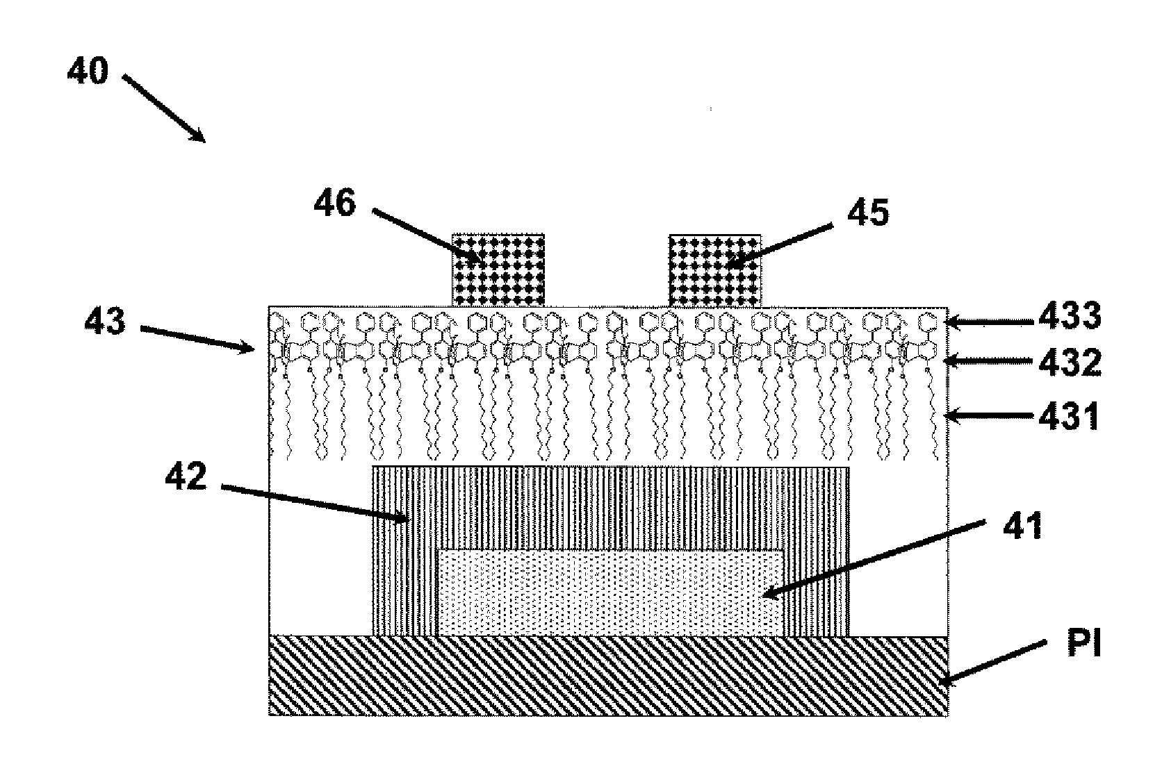
[0095]The use of the organic thin film of the present invention makes it possible to form an extremely uniform and clean interface between an organic semiconductor layer and an insulator layer, and thus it is possible to achieve an improvement in performance, homogeneity, and stability of an electronic device, in particular, an organic thin film transistor. Furthermore, it is possible to form a uniform electronic device, in particular, a transistor over a large area upon realizing a large-area flexible electronic device.
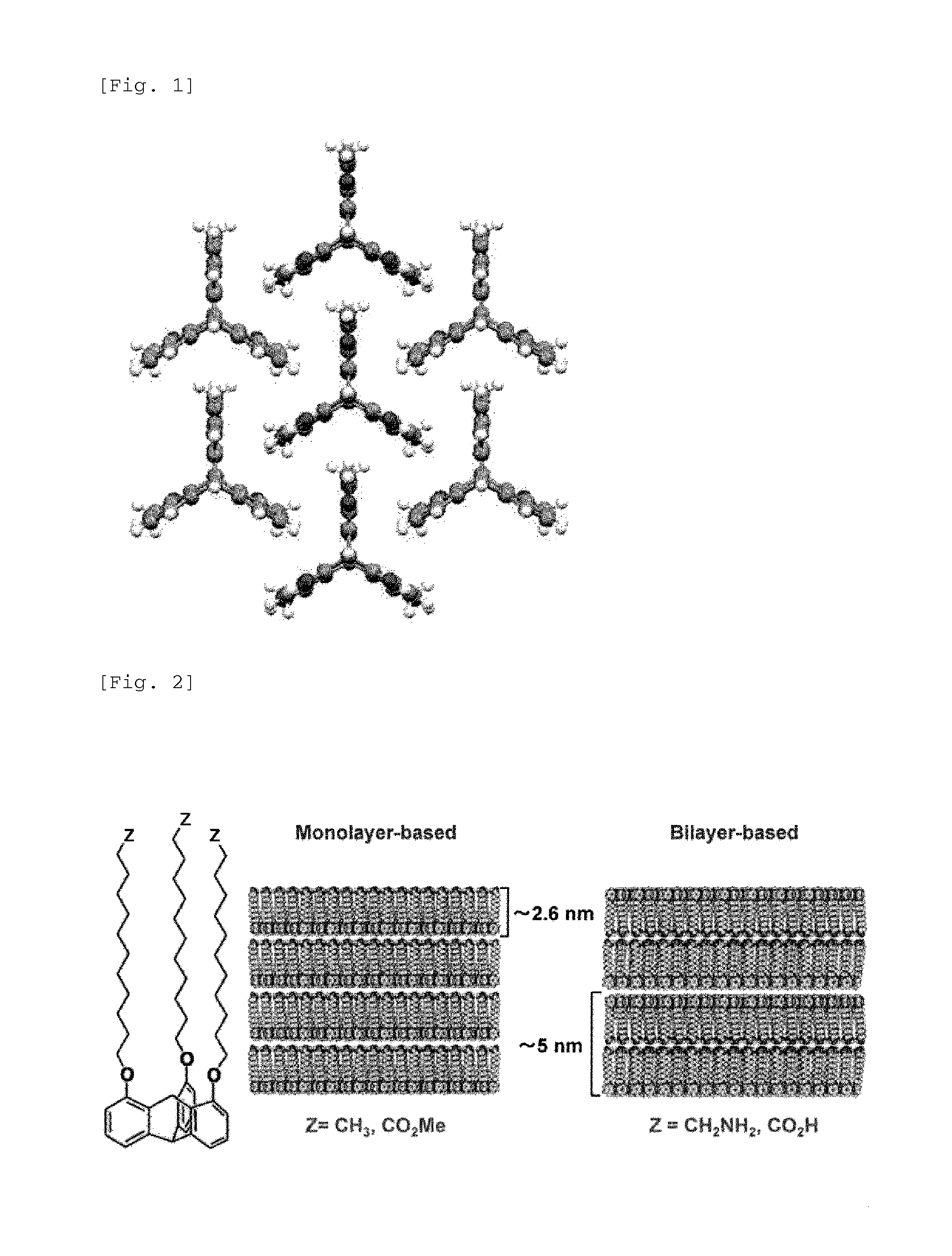
[0096]In addition, in another aspect of the present invention, a molecular moiety which functions as a semiconductor and a molecular moiety which functions as an insulator are incorporated in one molecule, and the molecule forms a monolayer. One side of the monolayer can exhibit semiconductor properties, and the other side can form a layered structure of insulator layers. This makes it possible to form an extremely homogeneous boundary between a semiconductor and an insulator and thus to realize a transistor wit

Problems solved by technology

At this time, the microscopic surface state of the insulator, in detail, surface roughness, substances adsorbed on the surface, surface molecular defect and the like affect the performance of the thin film transistor and significantly deteriorates the performance in many cases.
However, the solvent used in the coating method changes the nature of the surface of the insulator substrate and deteriorates the interface, and thus the organic thin film transistor fabricated have a decrease in performance such as an increase in driving voltage or an increase in leakage current in some cases.
However, the formation of the SAM on the surface of organic materials is limited.
Particularly, in the case of employing a metal oxide as an insulating layer to form an organic semic

Method used


Image

  • Electronic device using organic thin film, and electronic apparatus containing the same
  • Electronic device using organic thin film, and electronic apparatus containing the same
  • Electronic device using organic thin film, and electronic apparatus containing the same

Examples


Example

Production Example 1 Production of Trimethoxytriptycene Mixture Presented Below

[0217]

[0218]A suspension was prepared by adding acetonitrile (750 mL) to 1,8-dimethoxyanthracene (22.3 g, 93.7 mmol) and cesium fluoride (CsF) (85.3 mg, 561.0 mmol) and heated to 80° C. To this suspension, 2-methoxy-6-trimethylsilyloxy-trifluoromethylsulfonate (61.5 g, 188 mmol) was added dropwise, and the mixture was refluxed while heating for 5 hours. Acetonitrile was distilled off from the reaction mixture thus obtained under reduced pressure, the residue was washed with water and then a mixed solvent of hexane / chloroform (1 / 1, v / v), thereby obtaining intended trimethoxytriptycene (yield: 22.2 g, 64.5%). The trimethoxytriptycene thus obtained was revealed to be a mixture of 1,8,13-trimethoxytriptycene (Compound 5a) and 1,8,16-trimethoxytriptycene (Compound 5b) of 2:1 by the NMR measurement.

[0219]Compound 5a:

[0220]1H-NMR (400 MHz, CDCl3): δ(ppm)

7.01 (d, J=0.7 Hz, 3H), 6.90 (dd, J=7.3, 1.0 Hz, 3H), 6.80 ...

Example

Production Example 2 Production of 1,8,13-Trimethoxytriptycene (Compound 5a) Single Crystal

[0223]

[0224]The trimethoxytriptycene mixture (10.0 mg) produced in Production Example 1 was crystallized by dissolving in chloroform and allowing to stand, thereby obtaining 1,8,13-trimethoxytriptycene (2.0 mg) of the title.

[0225]The crystal thus obtained was subjected to the single-crystal X-ray structural analysis, and the result was as follows. This crystal had an orthorhombic crystal system, and the values of a, b, and c of unit cell were 15.608, 13.388, and 8.041, respectively in a unit of angstrom. The value of V was 1680 cubic angstrom.

Example

Production Example 3 Production of 1,8,13-Trihydroxytriptycene (Compound 6)

[0226]

[0227]To the trimethoxytriptycene mixture (22.0 g, 62.9 mmol) produced in Production Example 1, 320 mL of dichloromethane was added to prepare a suspension, and boron tribromide (BBr3) (18.2 mL, 192 mmol) was added to this, and the mixture was stirred for 4 hours at 0° C. To the reaction mixture, 200 mL of water was added, and the powder thus precipitated was collected by filtration and dried under reduced pressure. The powder thus obtained was dissolved in 80 mL of dimethylformamide, the mixture was allowed to stand at 5° C., and as a result, a colorless crystal was precipitated. This crystal was collected by filtration and washed with chloroform, thereby selectively obtaining 1,8,13-trihydroxytriptycene (Compound 6) (yield: 9.14 g, 71%) of the title.

[0228]Compound 6:

[0229]1H-NMR (400 MHz, acetone-d6): δ (ppm)

8.35 (br, s, 3H), 6.94-6.93 (d, J=7.2 Hz, 3H), 6.86 (s, 1H), 6.79-6.75 (dd, J=7.2, 0.9 Hz, 3H)...


PUM

PropertyMeasurementUnit
Dielectric polarization enthalpyaaaaaaaaaa
Structureaaaaaaaaaa
Molecular structureaaaaaaaaaa

Abstract

The present invention provides a high-performance, highly homogeneous, highly stable electronic device by forming an extremely uniform interface between an insulator and an organic semiconductor, as well as an electronic apparatus using the same. The present invention relates to an electronic device which contains, as a component, an organic thin film in which a geometric two-dimensional arrangement is formed regularly by interdigitating skeletal structures of a positive three-pronged shape of triptycene and by adding a first molecule extending out of one plane of a two-dimensional molecular structure of the triptycene skeletal structure. The invention also relates to an electronic apparatus and the like which contains the electronic device in the interior of the electronic apparatus.

Description

TECHNICAL FIELD[0001]The present invention relates to an electronic device including, as a component, a film that forms an extremely uniform interface between an insulator and an organic semiconductor, and a circuit board and an electronic apparatus containing the same.BACKGROUND ART[0002]In a thin film transistor using a semiconductor, a semiconductor thin layer is layered on the surface of an insulator and electrons or holes move through the semiconductor thin layer in the vicinity of this interface between the insulator and the semiconductor. In the case of an organic semiconductor material, the organic semiconductor material is heated to evaporate and attach the material to the surface of an insulator. At this time, the microscopic surface state of the insulator, in detail, surface roughness, substances adsorbed on the surface, surface molecular defect and the like affect the performance of the thin film transistor and significantly deteriorates the performance in many cases. In...

Claims


Application Information

Patent Timeline
IPC IPC(8): H01L51/00C07C43/21C07C43/215C07C43/225C07C69/734H01L49/02
CPCH01L51/0055C07C69/734C07C43/21C07C2103/90C07C43/225H01L28/40H01L51/0558C07C43/215C07C69/712C07C2603/86H10K85/60H10K10/484C07C2603/90H10K85/623
Inventor FUKUSHIMA, TAKANORISHOJI, YOSHIAKIISHIWARI, FUMITAKASEKITANI, TSUYOSHISOMEYA, TAKAO
Owner JAPAN SCI & TECH CORP
Why Eureka
Try Eureka