Material for electronic device and process for producing the same

a technology for electronic devices and materials, applied in the direction of semiconductor devices, basic electric elements, electrical appliances, etc., can solve the problems of increasing power consumption, accelerating deterioration of device properties, and deterioration of semiconductor device properties, so as to prevent deterioration of properties and excellent properties

Inactive Publication Date: 2006-03-02
TOKYO ELECTRON LTD
View PDF1 Cites 1 Cited by
  • Summary
  • Abstract
  • Description
  • Claims
  • Application Information

AI Technical Summary

Benefits of technology

[0020] The electronic device material constituted as above of the present invention can have excellent properties (for example, barrier property to boron) by virtue of a high N-atom concentration portion formed in the silicon oxynitride film constituting the electronic d

Problems solved by technology

However, if such an SiO2 film is merely made thin to 2.5 nm or less, the leak current passing through the gate insulating film (gate leak current) becomes large and this causes problems such as increase of power consumption or accelerated deterioration of device properties.
Furthermore, in using a conventional thin gate insulating film, boron contained in a gate electrode (mainly polysilicon) of a P-type MOS transistor penetrates into the SiO2 film at the formation of the gate electrode and the boron concentration of the gate electrode changes to cause a problem that the semiconductor device properties deteriorate.
However, the reduction of the channel length has the same meaning as the reduction in the area of MOS capacitor contained in that portion, namely, reduction in the capacitance, and this gives rise to an insufficient amount of carrier (electron or hole) induced at the operation and in turn, difficulty in obtaining an S/N ratio high enough to bring about the operation.
As the measure therefor, a method of decreasing the film thickness of the gate insulating film of FIG. 1 has been conventionally employed, but the thinning of the film incurs the following problems.
One problem is that a current (leak current) flows between the silicon substrate (channel) and the gate electrode due to quantum mechanical tunnel effect and the power consumption increases.
Also, with the thinning of the gate oxide film, as described abov

Method used


Image

  • Material for electronic device and process for producing the same
  • Material for electronic device and process for producing the same
  • Material for electronic device and process for producing the same

Examples


embodiment of

(One Embodiment of Production Apparatus)

[0082] One preferred embodiment of the production process of the present invention is described below.

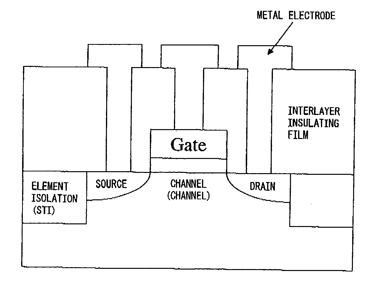
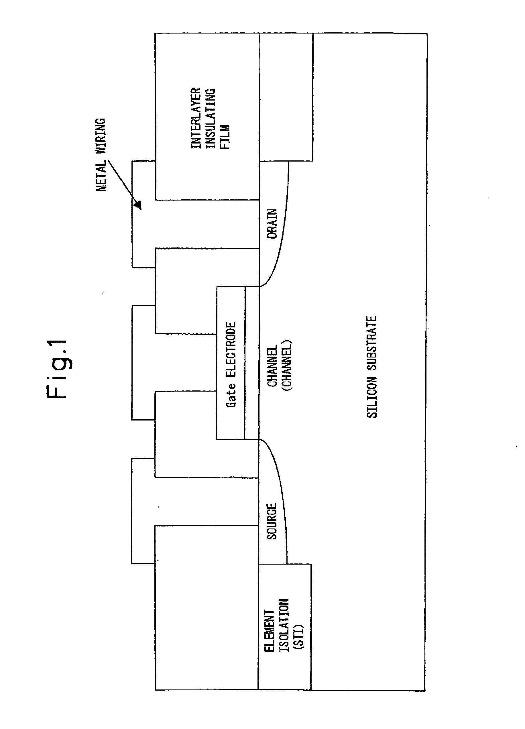
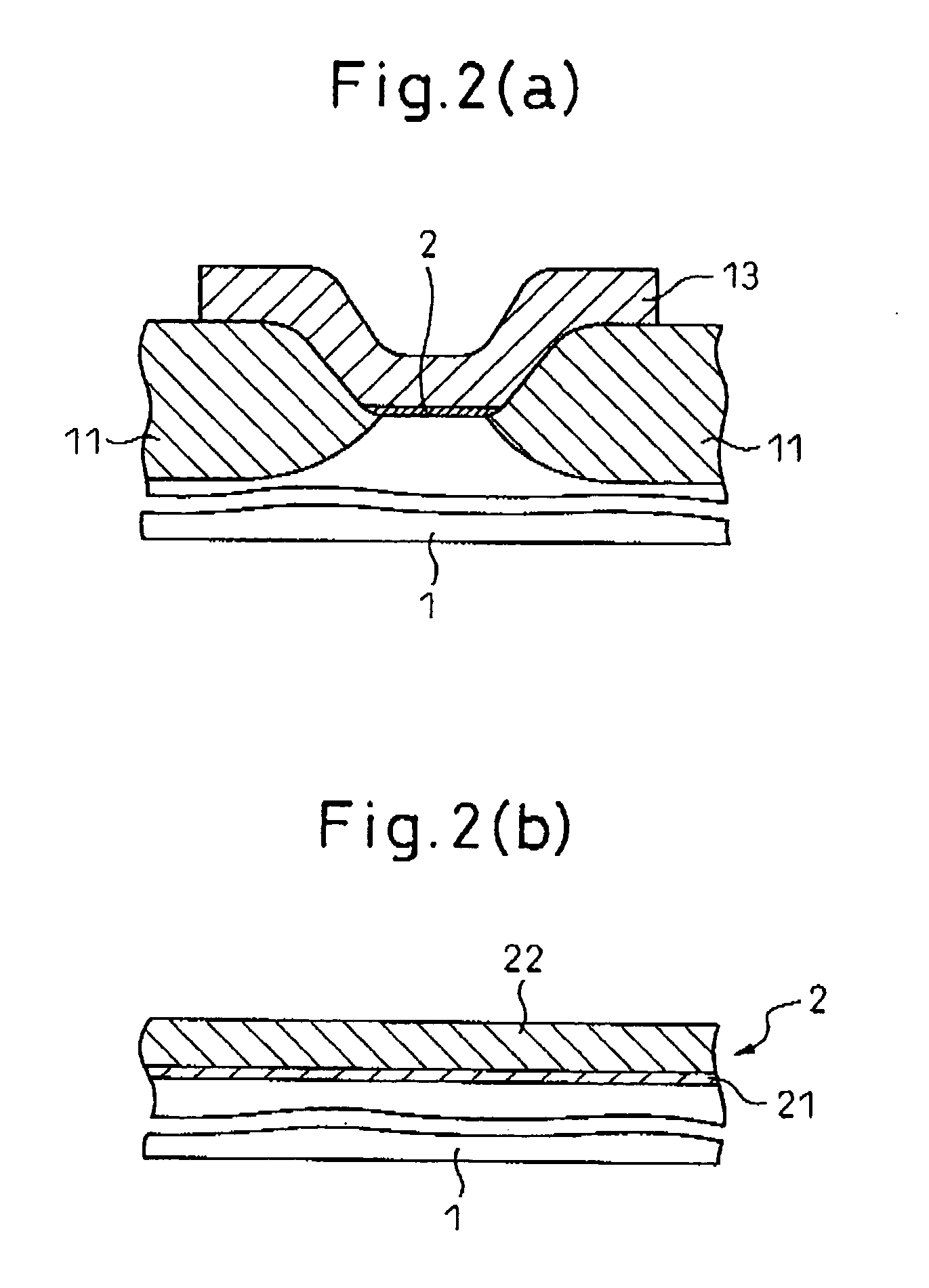
[0083] First, one example of the structure of a semiconductor device which can be produced by the production process of an electronic device material of the present invention is described by referring to FIG. 2 where the semiconductor device has an MOS structure using a gate insulating film as the insulating film.

[0084] Referring to FIG. 2(a), the reference numeral 1 in FIG. 2(a) is a silicon substrate, 11 is a field oxide film, 2 is a gate insulating film and 13 is a gate electrode. As described above, according to the production process of the present invention, a very thin and good-quality gate insulating film 2 can be formed. The gate insulating film 2 comprises, as shown in FIG. 2(b), a high-quality insulating film formed at the interface with the silicon substrate 1. For example, the gate insulating film is constituted by an oxide film...

example 1

[0114] The oxynitride film subjected to evaluation described later was produced through the following steps (1) to (7).

(1) Substrate

[0115] A 20-cm (8-inch) P-type or N-type silicon substrate having a resistivity of 8 to 12 Ωcm and a plane direction of (100) was used for the substrate.

(2) Washing before Gate Oxidation

[0116] A natural oxide film and contaminant factors (metal, organic material and particle) were removed by RCA washing where APM (a mixed solution of ammonia:aqueous hydrogen peroxide:pure water=1:2:10, 60° C.), HPM (a mixed solution of hydrochloric acid:aqueous hydrogen peroxide:pure water=1:1:10, 60° C.) and DHF (a mixed solution of hydrofluoric acid:pure water=1:100, 23° C.) were combined. In the RCA washing, APM: 10 minutes→pure water rinsing: 10 minutes→DHF: 3 minutes→pure water rinsing: 10 minutes→HPM: 10 minutes→pure water rinsing: 10 minutes→final pure water rinsing: 5 minutes were performed and thereafter, IPA (isopropyl alcohol, 220° C.) drying was perfor...

example 2

[0123] Samples treated until the step (4) above in Example 1 each was subjected to SIMS analysis to evaluate the nitrogen content in film. At the same time, the oxygen and silicon element were analyzed and from these results, the nitridation reaction was examined.

[0124] FIGS. 9 to 13 each shows the secondary ion mass spectrometry (SIMS) results of nitrogen atom when the thermal oxide film is subjected to the nitridation plasma treatment. The abscissa denotes the film thickness and the ordinate denotes the nitrogen content. The SIMS conditions used here were as follows.

[0125] Measuring apparatus: Physical-Electronics 6650 [0126] Primary ion species: Cs+[0127] Primary acceleration voltage: 0.75 KV [0128] Sputtering rate: about 9E-3 nm / sec [0129] Measurement region: diameter 420 μm×672 μm [0130] Degree of vacuum: 3E-7 Pa or less [0131] Measured ion polarity: +[0132] Charge-up compensation process: employed

[0133] The signal intensity of ion was converted into the concentration with u...


PUM


Abstract

An electronic device material comprising at least an electronic device substrate and a silicon oxynitride film disposed on the substrate is provided. The silicon oxynitride film is characterized by containing nitrogen atoms in a large amount in the vicinity of the oxynitride film surface when the nitrogen content distribution in the thickness direction of the silicon oxynitride film is examined by SIMS (secondary ion mass spectrometry) analysis. By virtue of this constitution, an electronic device material comprising an oxynitride film having an excellent effect of preventing penetration of boron and having excellent gate leak properties can be obtained.

Description

TECHNICAL FIELD [0001] The present invention relates to an electronic device material having an oxynitride film excellent in various properties (for example, barrier property to boron), and a production process thereof. The electronic device material and its production process of the present invention can be suitably used, for example, for forming a material for semiconductors or semiconductor devices (for example, those having an MOS-type transistor structure with a gate insulating film having excellent properties). BACKGROUND ART [0002] The present invention is widely applicable to the production in general of a material for semiconductors or electronic devices such as semiconductor device and liquid crystal device, but for the sake of convenience, the background art of semiconductor devices is described here as an example. [0003] With recent miniaturization of semiconductor devices, needs for a thin and good-quality silicon oxide film (SiO2 film) are significantly increasing. For...

Claims


Application Information

Patent Timeline
IPC IPC(8): H01L21/31H01L21/28H01L21/314H01L29/51
CPCH01L21/28202H01L29/518H01L21/3144H01L21/0214H01L21/0234H01L21/02332
Inventor SUGAWARA, TAKUYAOZAKI, SHIGENORISASAKI, NASARU
Owner TOKYO ELECTRON LTD
Why Eureka
Try Eureka