

Semiconductor composition
- Summary
- Abstract
- Description
- Claims
- Application Information
AI Technical Summary
Benefits of technology
Problems solved by technology
Method used
Image

Examples
example 1
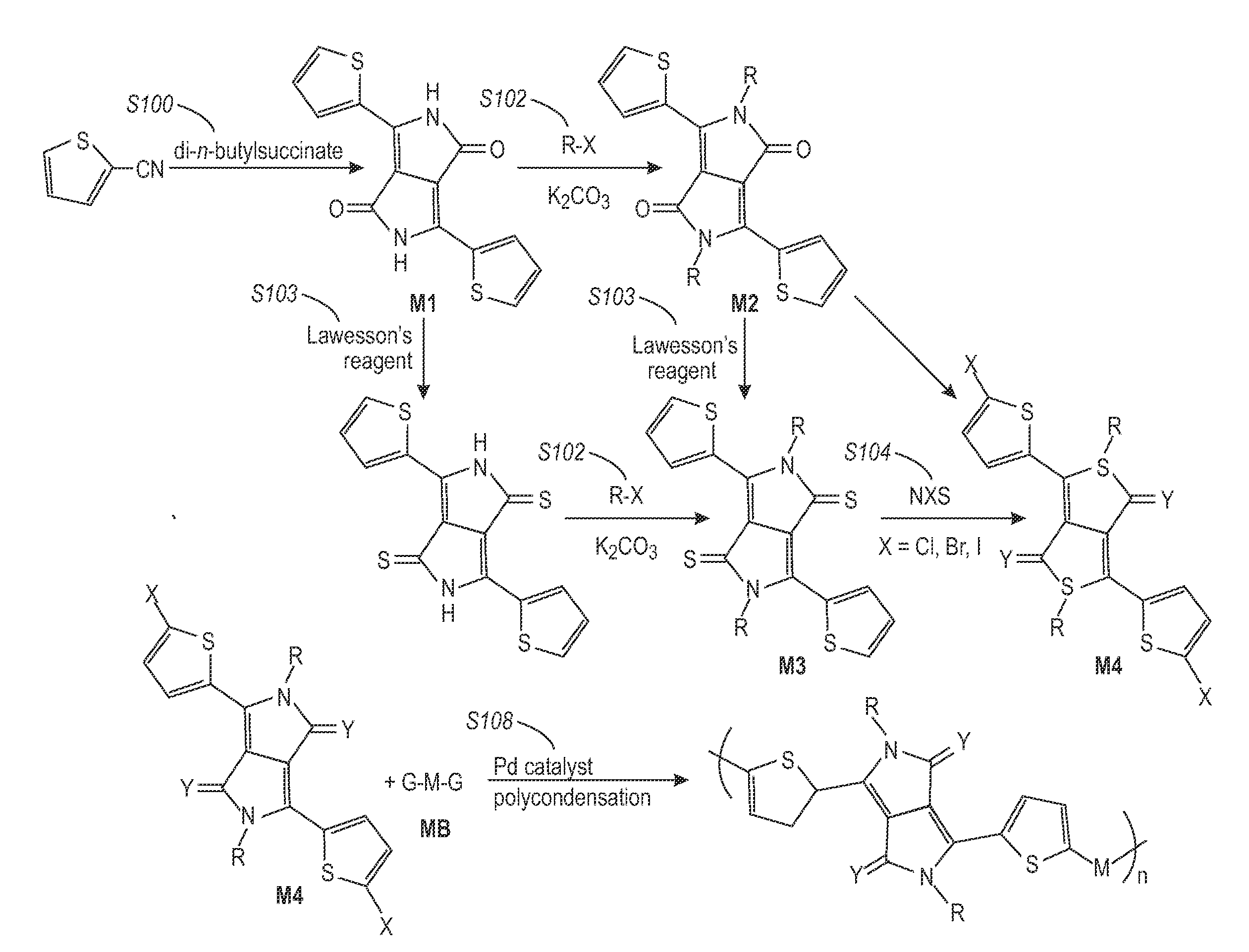
[0126]Poly(2,5-dioctadecyl-3,6-bis(thienyl-5-yl)-diketopyrrolopyrrole was synthesized as outlined in Scheme 1 below. This copolymer falls within Formula (I), Formula (II), and Formula (2) where Y1═Y2═O, R1═R2═C18H37, and R3═R4═H.
Synthesis of 3,6-Bis-(thienyl)-diketopyrrolopyrrole (1)
[0127]Sodium (3.45 grams, 0.15 mol) was added to 60 mL of t-amyl alcohol and a small amount of iron(III) chloride (50 mg) was added. The mixture was stirred vigorously for 1 hour at 95-102° C. until the sodium disappeared. The solution was cooled to 85° C. To the resultant solution was added 10.9 grams (0.1 mol) of 2-thiophenecarbonitrile. Then, 8.3 grams (0.04 mol) of diisopropyl succinate in 5 mL of t-amyl alcohol was added drop-wise over 1 hour at 85° C. When addition was complete, the mixture was maintained for 2 hours at this temperature. The reaction mixture was then cooled to 50° C., diluted with 50 mL of methanol, and then slowly neutralized with ˜15 mL of glacial acetic acid and refluxed briefly...
example 2
[0131]A diketopyrrolopyrrole-thiophene copolymer of Formula (A) (referred to hereafter as Polymer A) was synthesized:
[0132]In a 2-necked 100 mL round-bottomed flask 3,6-bis(5-bromothiophen-2-yl)-2,5-bis(2-octyldodecyl)pyrrolo[3,4-c]pyrrole-1,4(2H,5H)-dione (1.051 grams, 1.031 mmol) and 5,5′-bis(trimethylstannyl)-2,2′-bithiophene (0.507 grams, 1.031 mmol) were combined. The flask was fitted with a condenser and flushed with argon for 15 minutes. In a separate flask, anhydrous toluene was degassed by bubbling argon through the solvent for at least 30 minutes. The reactants were dissolved in anhydrous, deoxygenated toluene (25 mL) and the reaction was treated with Pd(PPh3)4 (0.060 grams, 0.052 mmol). The reaction mixture was then heated to an external temperature of 95° C. and stirred under an argon atmosphere. After 24 hours, the reaction mixture was treated with 2-bromothiophene (0.100 mL, 1.031 mmol) to end-cap the polymer chains. After 2 hours, the heating source was removed and th...
example 3
[0147]A diketopyrrolopyrrole-thiophene copolymer of Formula (B) (referred to hereafter as Polymer B) was synthesized in the similar manner as Polymer A:
[0148]10 mg of Polymer B was dissolved in 2 grams of 1,1,2,2-tetrachloroethane solvent with the assistance of heat and shaking to form a dark blue solution. The solution (0.5 wt % Polymer B) was stable at room temperature for days without precipitation.
[0149]A silicon wafer was provided as a substrate for an electronic device. Heavily doped silicon was used as a gate electrode. A 200-nm thick silicon oxide layer served as the gate dielectric layer. The surface of the silicon oxide layer was modified with octyltrichlorosilane.
[0150]After being filtered with a 0.2 micron syringe filter, the solution was spin coated at 2000 rpm onto the silicon wafer. A very smooth and shiny semiconducting film was obtained. After drying and annealing in a vacuum oven at 150° C. for 10 minutes, gold source / drain electrodes were vapor evaporated on top o...
PUM
| Property | Measurement | Unit |
|---|---|---|
| Fraction | aaaaa | aaaaa |
| Mass | aaaaa | aaaaa |
| Time | aaaaa | aaaaa |
Abstract
Description
Claims
Application Information