Display device and method of manufacturing the same

Active Publication Date: 2005-07-21
JAPAN DISPLAY CENT INC
View PDF3 Cites 0 Cited by
  • Summary
  • Abstract
  • Description
  • Claims
  • Application Information

AI Technical Summary

Benefits of technology

[0024] The present invention can provide a display device with driving elements capable of supplying mor

Problems solved by technology

In the case of an active matrix type light-emitting display device, however, the dispersion in grain diameters of the silicon crystals may cause the display device uneven brightness.
In the case of

Method used


Image

  • Display device and method of manufacturing the same
  • Display device and method of manufacturing the same
  • Display device and method of manufacturing the same

Examples


Example

Second Embodiment

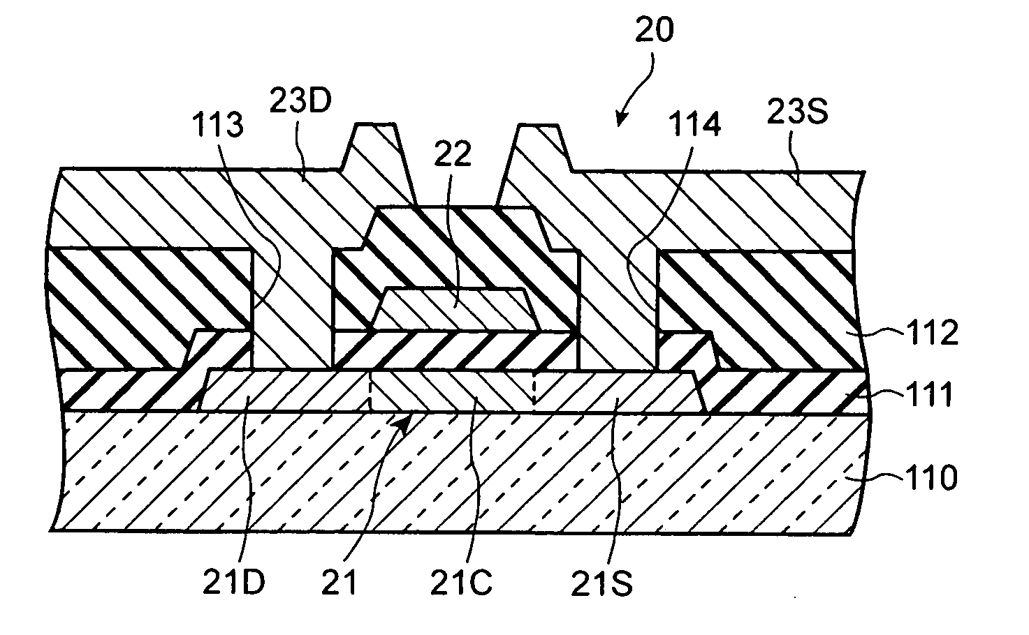
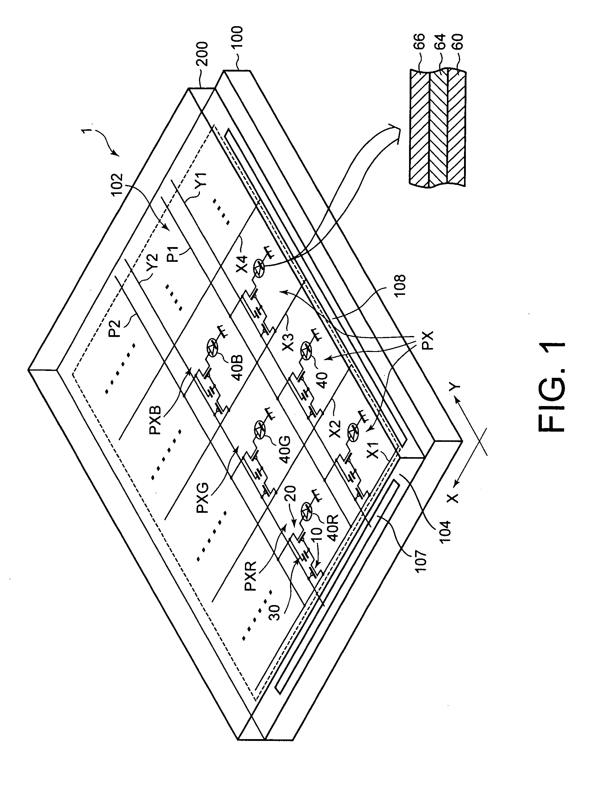
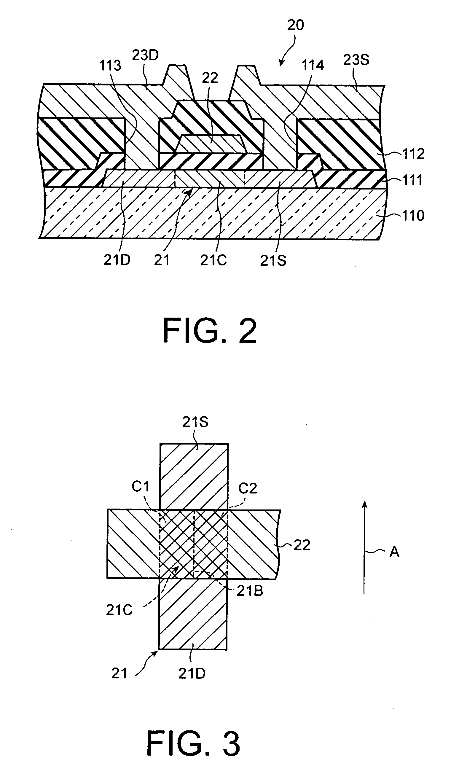
[0080] Next, a method of manufacturing semiconductor layer 21 of driving element 20 in accordance with the second embodiment of the present invention will be described below. However, detailed explanations of the same processes as in the first embodiment are omitted.

[0081] First,.an amorphous-silicon film-formed substrate is prepared. As schematically shown in FIG. 10, pulsed-laser beams are then irradiated to amorphous-silicon film a-Si and shifted by pitch LP in scanning (shot-moving) direction B.

[0082] As shown in FIGS. 10 and 11, poly-crystalline-silicon regions N, (N+1), (N+2), . . . are eventually formed by finally irradiated-laser-beam shots n, (n+1), (n+2), . . . , respectively. Width NW defined between adjacent poly-crystalline-silicon regions corresponds to laser-beam pitch LP. The width direction is consistent with scanning direction B of the laser beams.

[0083] Subsequently, as shown in FIG. 12, a patterning process is carried out for poly-crystalline...


PUM


Abstract

A display device includes a display area composed of pixels in a matrix. Each pixel has a light-emitting element and a driving element to supply a driving current to the light-emitting element. The driving element includes a thin film transistor with semiconductor layer 21 of a poly-crystalline film. Semiconductor layer 21 is provided with channel region 21C, and source and drain region 21S and 21D disposed on both sides of channel region 21C. Channel region 21C connects source region 21S to drain region 21D and has at least two conductive regions with different average grain sizes. Characteristics of the driving elements are made substantially uniform so that a display quality of the display device can be improved remarkably.

Description

CROSS-REFERENCE TO RELATED APPLICATIONS [0001] This application is based upon and claims the benefit of priority from the prior Japanese Patent Application No. 2003-398085, filed on Nov. 27, 2003, the entire contents of which are incorporated in this application by reference. FIELD OF THE INVENTION [0002] This invention relates to a display device and a method of manufacturing the same and, more particularly, to a light-emitting type display device with a light-emitting element provided for every pixel and a method of manufacturing the same. BACKGROUND OF THE INVENTION [0003] Recently, a light-emitting type flat panel display, such as an organic electroluminescence (EL) display device, has been widely noticed. Such an organic EL display device, for example, consists of a large number of pixels, each of which is provided with a fine organic EL display element. [0004] The organic EL display device has the following advantages: [0005] (1) Since the EL display element is a light-emittin...

Claims


Application Information

Patent Timeline
IPC IPC(8): H01L51/50G09F9/30G09G3/38H01L21/00H01L21/20H01L21/336H01L21/77H01L21/84H01L27/12H01L27/32H01L29/786H05B33/10H05B33/14
CPCH01L27/1285H01L27/1296H01L29/78696H01L29/78675H01L27/3262H10K59/1213H01L21/02675H01L29/78618
Inventor GOTO, YASUMASA
Owner JAPAN DISPLAY CENT INC
Why Eureka
Try Eureka