A light emitting die component formed by multilayer structures

a multi-layer structure and light-emitting die technology, applied in the direction of basic electric elements, electrical equipment, semiconductor devices, etc., can solve the problems of reducing quantum efficiency and thereby light output, stud-bumps interconnect approaches (related to functions iii and iv) can face serious heat-sinking limitations, existing fc die architectures generally present performance limitations in one or more of the seven previously listed essential functions, etc., to achieve high die area coverage, reduce hot spots and thermal resistan

Active Publication Date: 2015-12-17
LUMILEDS
View PDF6 Cites 15 Cited by
  • Summary
  • Abstract
  • Description
  • Claims
  • Application Information

AI Technical Summary

Benefits of technology

[0019]A further advantage is that the thermal spreading layer efficiently reduces hot-spots and thermal resistances inside the light emitting die component which improves the brightness and uniformity of the emitted light.
[0020]Another advantage is that the interconnect pad layout is completely decoupled from n-contact layer and / or p-contact layer, thus enabling compatibility with SMD like geometries. The latter generally includes as key parameter the gap distance between the p- and n-gaps. The wording gap distance should here be understood as the separation between the anode and cathode. The disclosed light emitting die structure enables the gap distance to be considerably large when needed without critically compromising the thermal performance of the die. This is possible due to the thermal spreading layer of high die area coverage.
[0021]According to an embodiment, when said second dielectric layer is arranged to electrically isolate said n-contact layer from said first region said n-contact layer comprises at least 20 vias per mm2 or when said second dielectric layer is arranged to electrically isolate said p-contact layer from said second region said p-contact layer comprises at least 20 vias per mm2. An advantage is that the current uniformity is improved.
[0022]The second dielectric layer may comprise benzocyclobutene, BCB, which is a reliable and low cost material that may be used due to the decoupled multilayer structure of the light emitting die component.

Problems solved by technology

Electrical power that is not converted into light emission from the LED converts into heat that must be conducted from the LED to its surroundings, since excess heat in the active region of the LED reduces quantum efficiency and thereby light output.
Existing FC die architectures generally present performance limitations in one or more of the seven previously listed essential functions.
For example, the stud-bumps interconnect approach (related to functions iii and iv) can confront serious heat-sinking limitations due to the reduced metal interconnect area.
Solutions for improved thermal performance has been disclosed but often is the architecture detriment of the die interconnection with submount and / or PCB, which becomes limited in terms of lacking compatibility with SMD technologies.

Method used


Image

  • A light emitting die component formed by multilayer structures
  • A light emitting die component formed by multilayer structures
  • A light emitting die component formed by multilayer structures

Examples


Embodiment Construction

[0031]The present invention will now be described more fully hereinafter with reference to the accompanying drawings, in which currently preferred embodiments of the invention are shown. This invention may, however, be embodied in many different forms and should not be construed as limited to the embodiments set forth herein; rather, these embodiments are provided for thoroughness and completeness, and fully convey the scope of the invention to the skilled person.

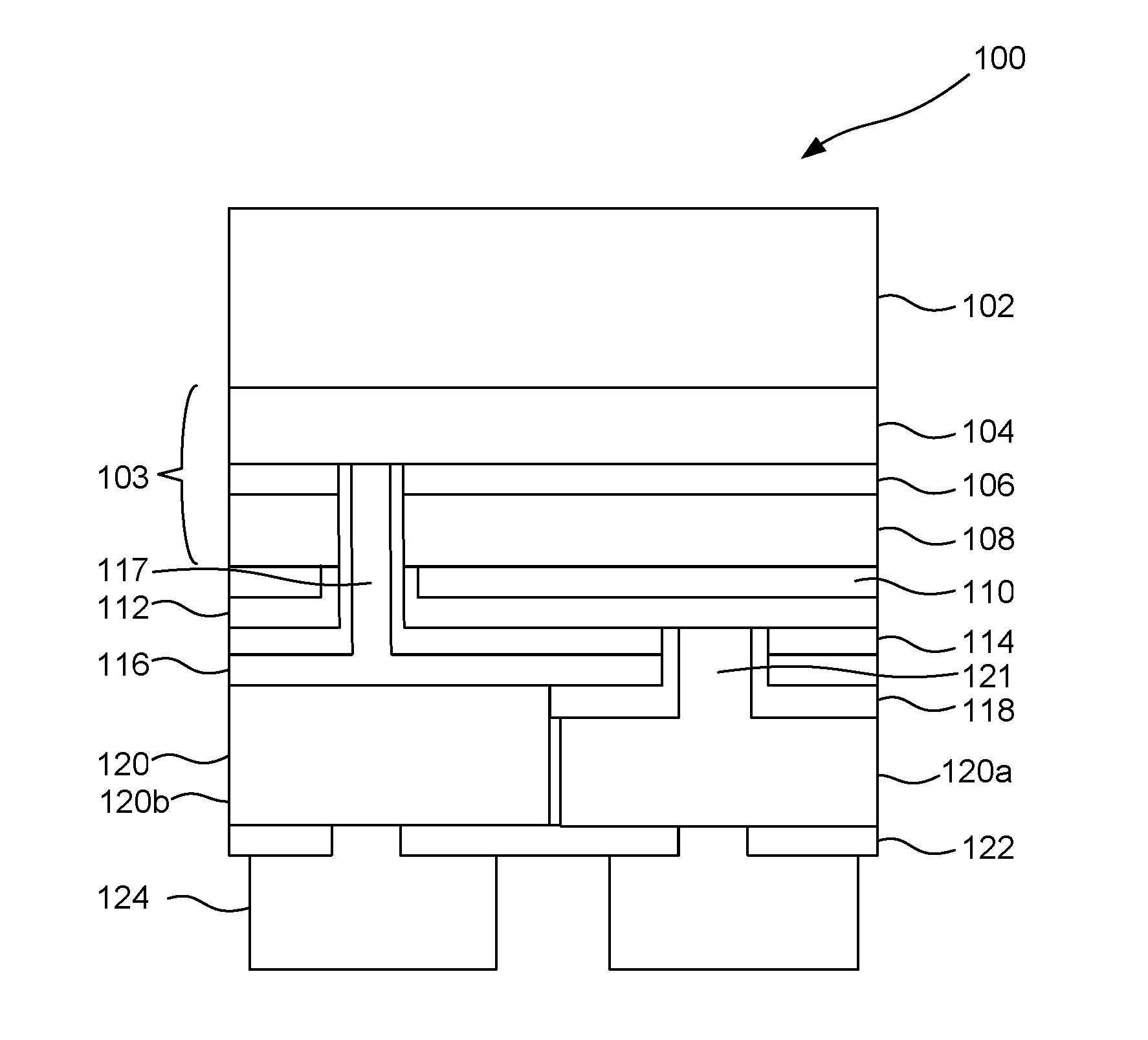
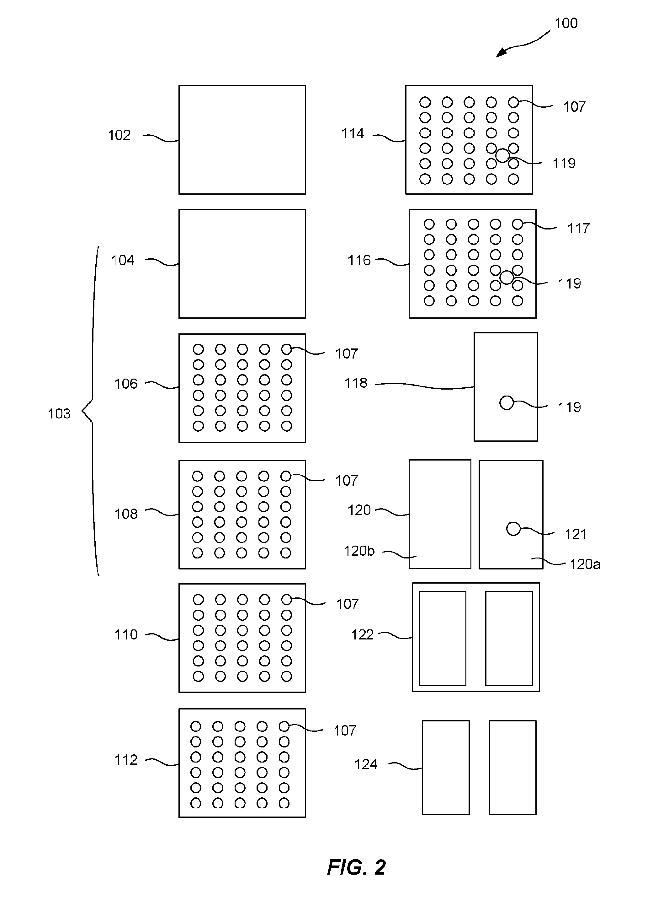
[0032]FIG. 1 shows a schematic cross sectional view of a first embodiment of a light emitting die component 100 according to the present invention. The light emitting die component comprises a substrate 102, a semiconductor structure 103 of GaN with an n-type layer 104, an active region 106, and a p-type layer 108, a p-contact layer 110 arranged to be in electrical contact with said p-type layer 108, a barrier layer 112 preventing migration of metal atoms, an n-contact layer 116 arranged to be in electrical contact with sai...


PUM


Abstract

The present invention relates to a light emit-ting die component formed by multilayer structures. The light emitting die component comprises a semiconductor structure (103) comprising: an n-type layer (104), an active region (106) and a p-type layer (108); a p-contact layer (110) arranged to be in electrical contact with said p-type layer (108); an n-contact layer (116) arranged to be in electrical contact with said n-type layer (104); a first dielectric layer (114) arranged to electrically isolate said p-contact layer (110) from said n-contact layer (116); a thermal spreading layer (120) comprising a first and a second region (120a, 120b) being electrically isolated from each other, wherein said first region (120a) forming an anode electrode of said light emitting die component and said second region (120b) forming a cathode electrode of said light emitting die component; a second dielectric layer (118) arranged to electrically isolate said n-contact layer (116) from said first region (120a) or to electrically isolate said p-contact layer (110) from said second region (120b); a third dielectric layer (122) arranged to electrically isolate said first and second regions (120a, 120b); and an interconnect pad (124) enabling interconnection with a submount (126).

Description

FIELD OF THE INVENTION[0001]The present invention relates to a light emitting die component formed by multilayer structures for improved device performance.BACKGROUND OF THE INVENTION[0002]Solid state light sources such as light emitting diodes (LEDs) are among the most efficient light sources available today. LEDs provide longer lifetime, higher photon flux efficacy, lower operating voltage, narrow-band light emission, and flexibility in terms of assembly compared to conventional light sources.[0003]Commonly, III-V semiconductor materials are used to provide high-brightness light emitting devices operating in the ultraviolet, visible or infrared regions of the electromagnetic spectrum. The materials used include for example binary, ternary and quaternary alloys of gallium, aluminum, indium, nitrogen, phosphorus and arsenic.[0004]Gallium nitride (GaN) LEDs have recently attracted much attention as efficient light sources, where the combination of GaN with In (InGaN) or Al (AlGaN) fu...

Claims


Application Information

Patent Timeline
Patent Type & Authority Applications(United States)
IPC IPC(8): H01L33/64H01L33/38
CPCH01L33/647H01L33/641H01L33/382H01L33/486H01L33/62H01L2924/0002H01L2924/00
Inventor LOPEZ, TONI
Owner LUMILEDS
Why Eureka
Try Eureka