Substrate panel

Inactive Publication Date: 2010-02-18
POWERTECH TECHNOLOGY
View PDF6 Cites 2 Cited by
  • Summary
  • Abstract
  • Description
  • Claims
  • Application Information

AI Technical Summary

Benefits of technology

[0021]Furthermore, as shown in FIG. 2, the frame 241 and the current input lines 221 are perpendicularly intersected to form a plurality of right angles. As shown in FIG. 2 again, the frame 241 can equally divide the current input lines 221, i.e., the length of one portion of the current input lines 221 from the frame 241 to the substrate strips 210A is equal to the one of another portion of the current input lines 221 from the frame 241 to the current input side 201 of the substrate panel 200. Furthermore, the length of the current output lines 222 from the frame 241 to the substrate strips 210 may also be equal to the one of the current output lines 222 from the frame 241 to the current output side 202 of the substrate panel 200. In the present embodiment, as shown in FIG. 2, the meshes 242 and the cascaded lines 230 are perpendicularly intersected. In the present embodiment, as shown in FIG. 2, the meshes 242 can equally divide the cascaded lines 230, i.e., the lengths of two portions of the cascaded lines 230 located at two corresponding sides of the meshes 242 are equal to achieve evenly distributing the plating current. Preferably, as shown in FIG. 2, the current input buffer gate 240 further has a plurality of plating distributing lines 243 to connect the frame 241 to the adjacent substrate strips 210A to enhance the uniformity of the current distribution. The plating distributing lines 243 may not connect to current input side 201 of the substrate panel 200. The plating distributing lines 243 and the current input lines 221 are parallelly disposed at a same side of the substrate strips 210A with equal spacing to achieve better input current distributions. Preferably, more current distributing lines 243 and the current output lines 222 are parallelly disposed so that all of current distributing lines 243 are arranged only adjacent to the current input side 201 and the current output side 202. The side rails of the substrate panel 200 between the sides 201 and 202 has no plating distributing lines connecting from the frame 241 to the near row of the substrate strips 210A so that the current distributed in the frame 241 will flow to farther rows of the substrate strips 210 through the meshes 242 instead of the near row of the substrate strips 210A where high current densities are easily accumulated. Hence, the frame 241 can provide better current buffers and reduce the edge effects.
[0022]Preferably, as shown in FIG. 4A, the substrate panel 200 further has a plating layer 250 such as Ni/Au formed on the frame 241 by electroplating, i.e., the frame 241 is not covered by solder masks 260. In the present embodiment, a plating layers 250 can further be formed on the frame 241. During electropla

Problems solved by technology

Moreover, poor plating qualities will cause wire-bonding failure or poor

Method used


Image

  • Substrate panel
  • Substrate panel
  • Substrate panel

Examples


Example

[0014]Please refer to the attached drawings, the present invention is described by means of embodiment(s) below.

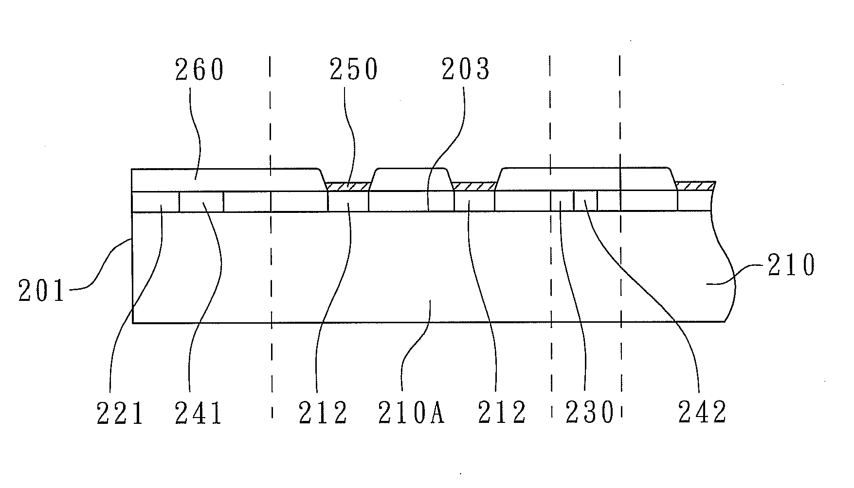
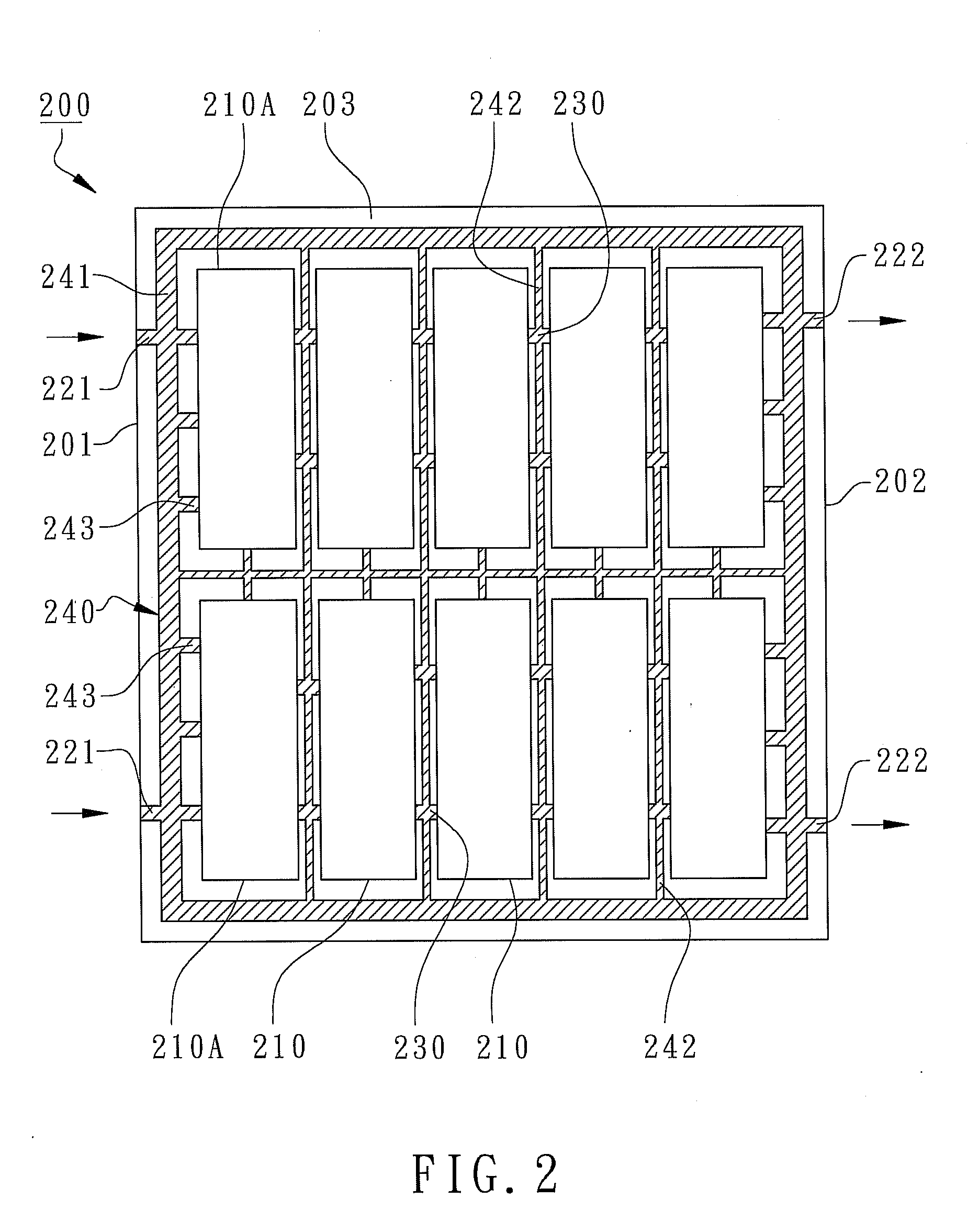
[0015]According to the preferred embodiment of the present invention, a substrate panel is illustrated in the top view of FIG. 2 and the partially cross-sectional view of FIG. 4A.

[0016]The substrate panel 200 primarily comprises a plurality of substrate strips 210, one or more current input lines 221, a plurality of cascaded lines 230, and a current input buffer gate 240. Normally, the substrate panel 200 is a large-dimension printed circuit board with the length equal to or less than twice of the width such as 1:1, 4:3, or 16:10.

[0017]The substrate strips 210 are integrally connected in the substrate panel 200 and are arranged in an array. The integral connection means that all of the substrate strips 210 share a same core layer and circuit layer(s) of the substrate panel 200. As shown in FIG. 3, each substrate strip 210 includes a plurality of substrate units 211 arrange...


PUM


Abstract

A substrate panel primarily comprises a plurality of substrate strips arranged in an array, one or more current input lines, a plurality of cascaded lines connecting between the substrate strips, and a current input buffer gate. Current input lines connect a current input side of the substrate panel to the adjacent substrate strips. The current input buffer gate has a frame around the substrate strips and a plurality of meshes where the frame intersects with the current input lines and the meshes intersect with the cascaded lines with both ends of the meshes connecting to the frame. Therefore, the current can be evenly distributed to each substrate strip during plating processes to improve the issues of different plating thicknesses and different plating roughness caused by different current densities and to protect the internal circuits inside the substrate strips from the damages due to current surges and unstable voltages.

Description

FIELD OF THE INVENTION[0001]The present invention relates to a printed circuit board, and more particularly to a substrate panel including a plurality of substrate strips for semiconductor packages.BACKGROUND OF THE INVENTION[0002]Printed circuit boards have been implemented as micro substrates or substrate units for carrying chips in semiconductor packages. A plurality of micro substrates are arranged in an array and disposed on a substrate strip where the semiconductor packages are assembled on the substrate strip. Furthermore, a plurality of substrate strips are arranged on a substrate panel for mass production by the processes of printed circuit boards. Normally, before the singulation of a substrate strip, nickel / gold or other metals are electroplated on the metal pads on the substrate panel to prevent metal oxidation and to enhance metal bonding strengths in the following processes such as wire bonding or solder ball placement.[0003]As shown in FIG. 1, a conventional substrate...

Claims


Application Information

Patent Timeline
IPC IPC(8): H05K1/02
CPCH05K3/0052H05K2201/09254H05K3/242
Inventor FAN, WEN-JENG
Owner POWERTECH TECHNOLOGY
Why Eureka
Try Eureka