Package-on-package semiconductor assembly

a technology of semiconductor assemblies and packaging, applied in the direction of semiconductor devices, semiconductor/solid-state device details, electrical apparatus, etc., can solve the problems of assembly with different thermal properties, assembly with thin assemblies, and assemblies with thin layers, etc., to achieve the effect of reducing warping and increasing robustness

Active Publication Date: 2010-03-09
TEXAS INSTR INC
View PDF23 Cites 114 Cited by
  • Summary
  • Abstract
  • Description
  • Claims
  • Application Information

AI Technical Summary

Benefits of technology

[0005]In carrying out the principles of the present invention, in accordance with preferred embodiments thereof, POP IC assemblies are provided with improved components and methods to increase robustness and reduce warping.
[0008]According to yet another aspect of the invention, a POP semiconductor assembly has a first packaged device which includes a substrate with a surface for accepting a chip. The substrate surface also has electrical contacts for external connection. A chip affixed to the substrate surface and electrically coupled to the contacts is enclosed in an encapsulated region defined by the substrate surface. The encapsulated region also includes contact apertures for permitting external communication with the contacts. A second packaged device is affixed to the encapsulated region of the first package and operably coupled to the contacts such that the devices can function in concert.

Problems solved by technology

One of the challenges of POP technology lies in minimizing thickness.
A particular problem for POP implementation is posed by the inherent conflict between the need to minimize thickness and the need to minimize and withstand warpage.
Warpage can lead to some of the most common and debilitating problems encountered by semiconductor assemblies such as the separation of solder joints, fractures, the separation of layers, and open or short circuits caused by the separation of materials, or by the ingress of moisture between separated materials.
Thin assemblies, and assemblies with layers that have differing thermal properties, e.g. POP assemblies, are particularly susceptible to warping.
Warpage is generally most severe in the non-molded areas of conventional packages, i.e. the edges, and especially the corners.

Method used


Image

  • Package-on-package semiconductor assembly
  • Package-on-package semiconductor assembly
  • Package-on-package semiconductor assembly

Examples


Embodiment Construction

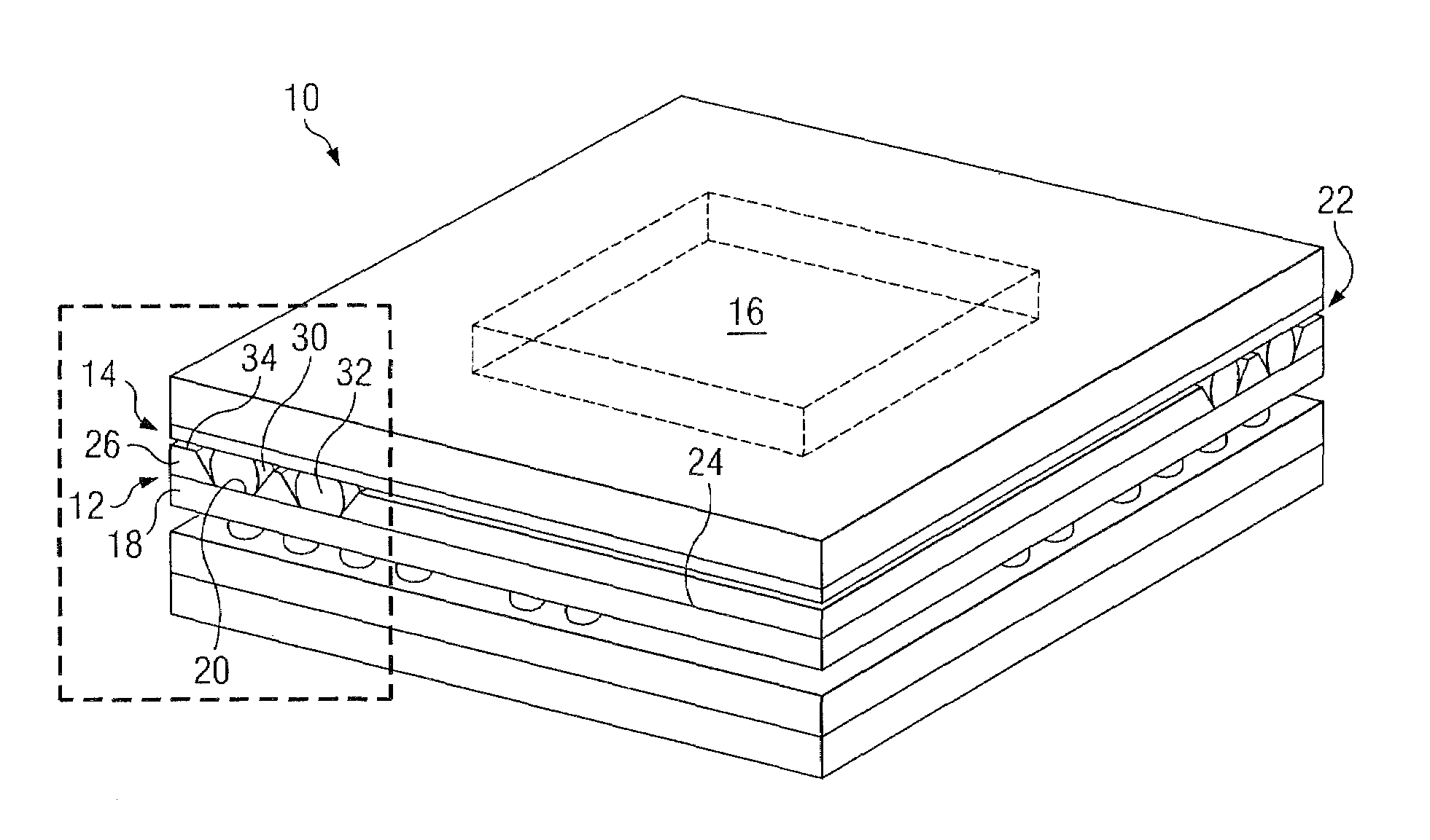
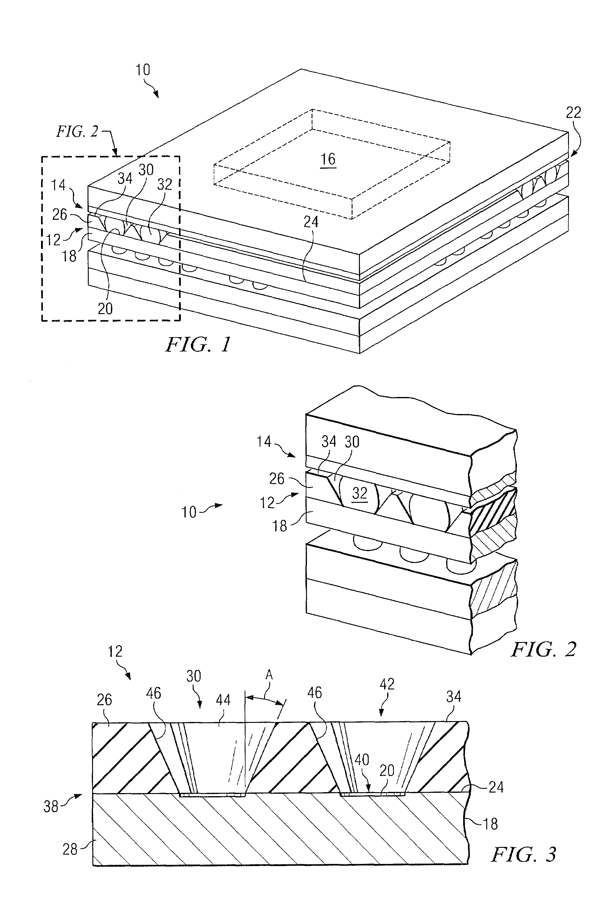
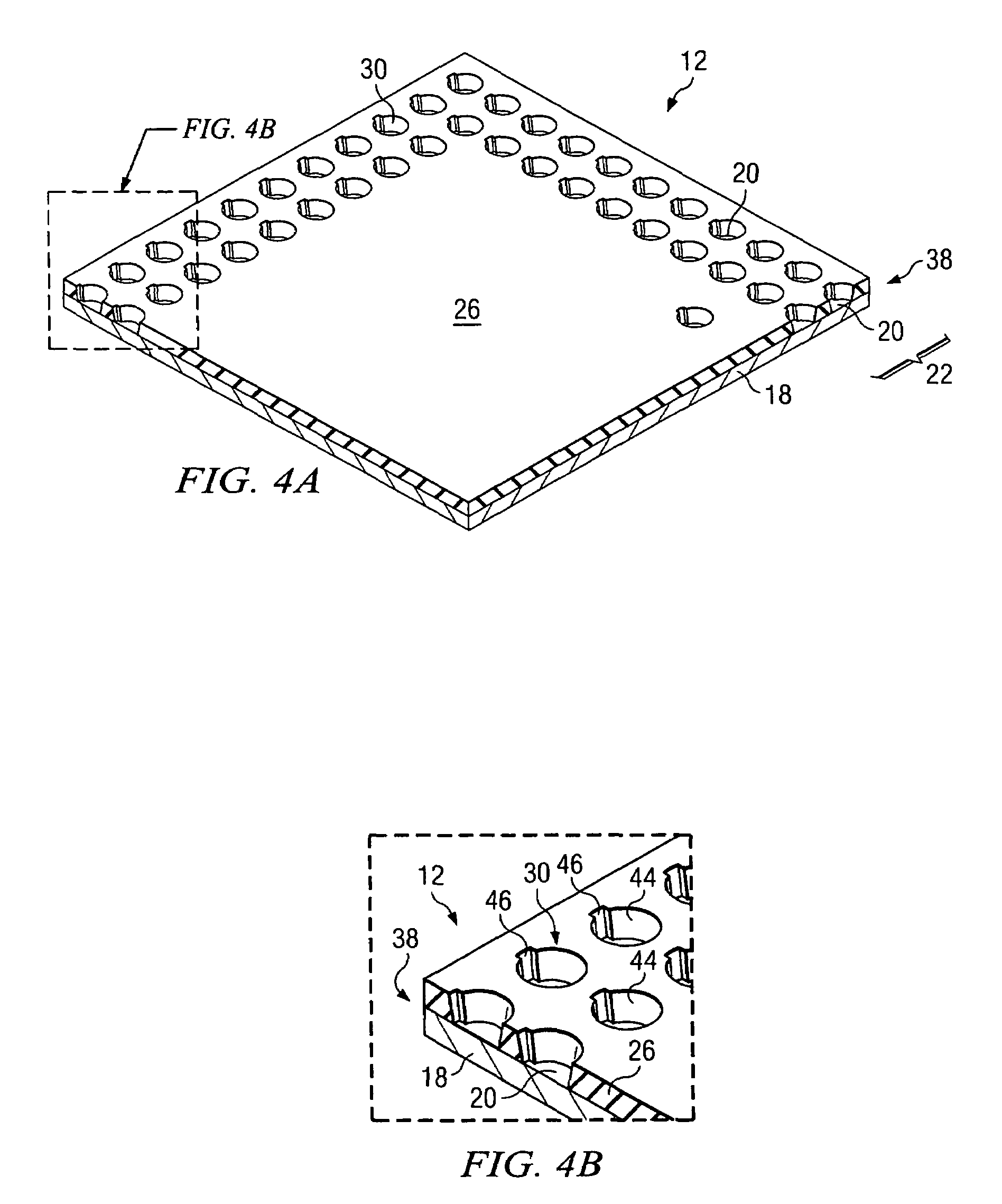
[0022]A POP assembly 10 is shown in the partial cutaway views of FIGS. 1, 2 and 3. A bottom package 12 is affixed to a top package 14 in a configuration to form a completed POP assembly 10 according to a preferred example of the invention. It should be understood that each package 12, 14, may include a chip 16 affixed to a substrate 18 having leads or pads 20 for making electrical connections as is known in the arts. It should also be understood that the terms “bottom” and “top” are used herein to describe the arrangement of the components as shown in the drawings and are not intended to delimit or restrict the spatial relationship of the components in any absolute sense, for example, the POP assembly 10 shown and described could be rotated in any direction or overturned without altering the invention. Typically, the chip 16 is more-or-less centrally located and the leads or contact pads 20 are located at or near the periphery 22 of the substrate 18 surface 24. The chip 16 is encaps...


PUM


Abstract

Disclosed are methods and devices for providing improved semiconductor packages and POP IC assemblies using the improved packages with reduced warping. According to disclosed embodiments of the inventions, a packaged semiconductor device for use in a POP assembly includes an encapsulated region generally defined by the substrate surface. The encapsulant is provided with contact apertures permitting external communication with contacts on the substrate and coupled to an encapsulated chip. Preferred embodiments of the invention are described in which the contact aperture sidewalls are angled within the range of approximately 10-30 degrees or more from vertical and in which the contact aperture is provided a gas release channel to permit gas to escape during reflow.

Description

TECHNICAL FIELD[0001]The invention relates to semiconductor assemblies. More particularly, the invention relates to package-on-package (POP) integrated circuit (IC) assemblies and methods for manufacturing the same.BACKGROUND OF THE INVENTION[0002]Package-on-Package (POP) stacking of semiconductor devices is known in the arts. Stacking packages offers significant advantages primarily related to reducing device footprints. It can also be used to improve testability, for example by permitting separate testing of logic and memory packages before they are assembled in a stacked POP unit. In some instances, electrical performance may also be improved due to shortened interconnections between associated packages. Conventional POP designs are generally similar to BGA devices. A bottom package has a substrate with a top surface having a more-or-less centrally located encapsulated area containing enclosed circuitry. The encapsulated area is typically bordered by an unencapsulated periphery b...

Claims


Application Information

Patent Timeline
Patent Type & Authority Patents(United States)
IPC IPC(8): H01L25/11
CPCH01L23/49827H01L25/105H01L2924/3511H01L2225/1023H01L2924/0002H01L2225/1058H01L2924/00
Inventor GERBER, MARK ALLENO'CONNER, SHAWN MARTIN
Owner TEXAS INSTR INC
Why Eureka
Try Eureka